Speakers
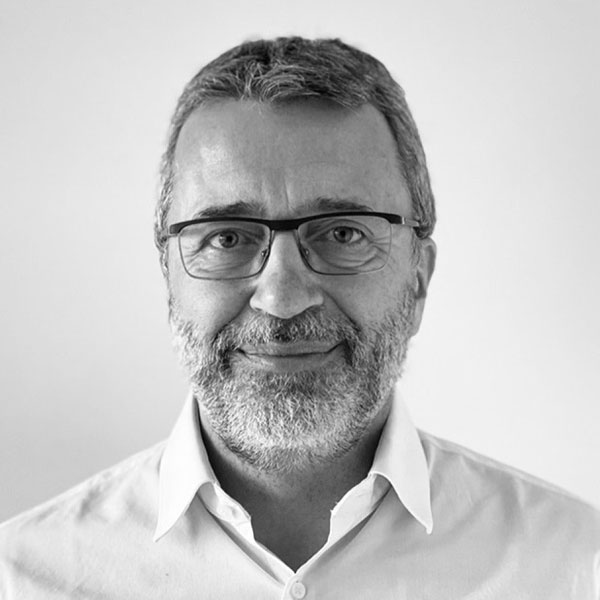
Gregg Bartlett
CTO, GlobalFoundries
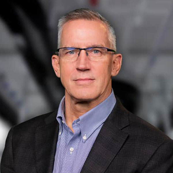
Gregg Bartlett
CTO, GlobalFoundries
Bio:
Gregg Bartlett is Chief Technology Officer for GF, a position he was appointed to in 2022. He leads the execution and delivery of the company’s differentiated technology roadmap, including partnering with key universities and institutions to drive innovation, and accelerating development and delivery of GF’s differentiated technology. Mr. Bartlett oversees technology development, design enablement, GF Labs and global reliability and technology solutions.
Prior to his current role, Mr. Bartlett was Senior Vice President of Technology, Engineering and Quality at GF from 2019 to 2022. Before that, he served in various senior executive roles at GF including Head of Technology Development, Chief Technology Officer and Head of the CMOS (complementary metal-oxide-semiconductor) business from 2009 to 2019. Before joining GF, Mr. Bartlett spent 25 years in technical and management positions at Freescale Semiconductor and its predecessor, Semiconductor Products Sector at Motorola. Mr. Bartlett currently serves as a member of the board directors of Carbice Corporation.
Mr. Bartlett holds a bachelor’s degree in Chemical Engineering from Kansas State University.
Abstract:
The IoT/Edge Compute Era has ushered in an order of magnitude increase in connected devices each year compared to
smart mobile devices. With this comes great challenges in processing data at the edge with connected devices, the need
for intelligence and security in those devices, all with an eye toward sustainability. These formidable challenges create great
opportunities for innovation. For semiconductor foundries, this is the first compute era not dominated by single digit
nanometer technology, rather by creating compelling features on existing technologies to enable this connected, intelligent
and power efficient ecosystem. Building that ecosystem requires great R&D partnerships to deliver on the promise of this
future world
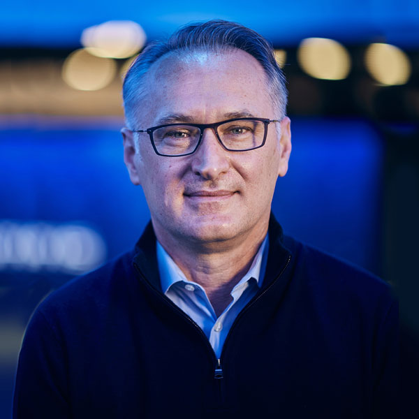
Ned Curic
CTO, Stellantis
Ned Curic
CTO, Stellantis
Bio:
Ned Curic was appointed Chief Technology Officer and a member of Stellantis’ Top Executive Team on August 30, 2021. From June 2017, Ned Curic was Vice President, Alexa Automotive at Amazon spearheading Amazon’s efforts in the Automotive industry. Ned Curic started his career in 1996 in the field of Engineering Systems at Northrop Grumman, an American multinational aerospace and defense technology company. After a short stint in the financial industry, in 2000 he joined Microsoft where he held various roles in Consulting, Product, Security and Advisory. He entered the automotive sector in 2013, as Group Vice President & Chief Technology Officer at Toyota Motor North America and, in 2015, became Co-founder and Executive Vice-President, Technical Director and Board Member at Toyota Connected. Ned Curic studied Informatics and Computer Science, and received a Master’s in Business Administration (Pepperdine University, George L. Graziadio School of Business and Management) in 2012.
Abstract:
Technologies have the power to reshape the auto industry, change the way we experience mobility and, ultimately, transform our life and our society. In guiding this transformation, we need to make sure that we don’t develop tech for tech’s sake but rather a tech made for real people, designed around their needs, delightful and easy to enjoy, whose impact is also fair, respectful of the environment and sustainable.
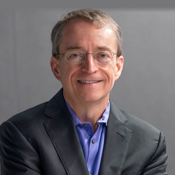
Pat Gelsinger
CEO, Intel
Pat Gelsinger
CEO, Intel
Bio:
Patrick (Pat) Gelsinger is chief executive officer of Intel Corporation and serves on its board of directors. He has more than four decades of technology leadership and experience driving innovation, with 30 of those years serving in Intel engineering and executive roles.
Before rejoining Intel in February 2021, Gelsinger was CEO of VMware. In that role, he transformed VMware into a recognized global leader in cloud infrastructure, enterprise mobility and cybersecurity – almost tripling the company’s annual revenues. Gelsinger was also ranked the top CEO in America in 2019 in Glassdoor’s annual employee survey. Prior to joining VMware in 2012, Gelsinger was president and chief operating officer of EMC’s Information Infrastructure Products business, overseeing engineering and operations for information storage, data computing, backup and recovery, RSA security and enterprise solutions.
Gelsinger began his career in 1979 at Intel, becoming its first chief technology officer and serving as senior vice president and the general manager of the Digital Enterprise Group. He managed the creation of key industry technologies like USB and Wi-Fi. He was the architect of the original 80486 processor, led 14 microprocessor programs and played key roles in the Intel® Core™ and Intel® Xeon® processor families, leading to Intel becoming the world’s preeminent microprocessor supplier.
Gelsinger earned degrees in electrical engineering: an associate degree from Lincoln Technical Institute, a bachelor’s degree from Santa Clara University and a master’s degree from Stanford University. He was elected a member of the National Academy of Engineering in February 2023. Gelsinger holds eight patents in the areas of VLSI design, computer architecture and communications, is an IEEE Fellow, and serves as a member of the National Security Telecommunications Advisory Committee. He also sits on the Business Council, Business Roundtable, CEO Council, CEO Forum, Global Semi Alliance, Tech Council CEO and U.S. Chamber China Center Advisory Board.
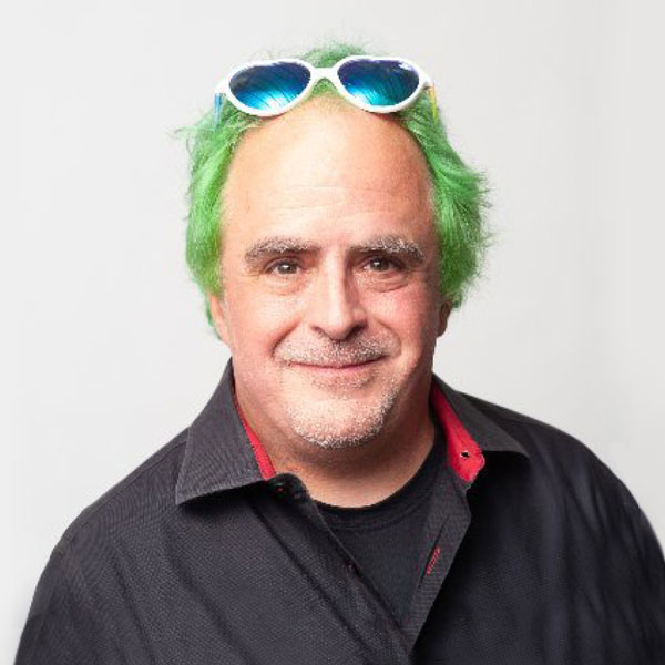
David Andre
Chief Science Officer, Google X
David Andre
Chief Science Officer, Google X
Bio:
Dave is a scientist, inventor, and entrepreneur whose work emphasizes the role of machine learning and AI, especially with respect to time-series data, search and optimization in program space, and decision making under uncertainty. He is Chief Science Officer at X and runs a team of mathematicians and machine learning experts working on early stage projects. He co-founded several companies, including Cerebellum Capital, which was an asset management company powered by an auto-ML system that discovered trading strategies. He also invested in and advised a number of startups in the data science and wearables space. He previously worked at Bodymedia, where he ran the machine learning team and several advanced development projects. Over the years, he’s helped start a number of other businesses. Personally, he’s a husband, father, snowboarder, passionate player of soccer and bridge, a puzzle nerd, a burner, and a travel-lover. He runs robot & programming clubs for his two kids to help them & friends get a deeper tech education. He got started down his path at Stanford University (1994: BS Symbolic Systems, BA Psychology) and completed his official education at UC Berkeley (2003: PhD EECS with a focus on Artificial Intelligence). He feels very lucky to have been interested in AI & ML well before it was cool.
Abstract:
The field of artificial intelligence is changing at a breakneck pace, revolutionizing many industries along the way, including software engineering and many elements of artistic creation. In addition to briefly introducing X (formerly Google X), this talk will discuss these trends and implications for hardware design, both in terms of how AI can fit into the design process as well as what changes could supercharge these coming applications.
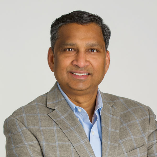
Mukesh Khare
GM IBM Semiconductors & VP Hybrid Cloud Research, IBM
Mukesh Khare
GM IBM Semiconductors & VP Hybrid Cloud Research, IBM
Bio:
Dr. Mukesh V. Khare is General Manager of IBM Semiconductors division and Vice President of Hybrid Cloud research. He leads a global team of more than 1000 researchers and engineers that are re-defining the future of computing for next generation workloads such as generative artificial intelligence (AI), high-performance computing, and their delivery via hybrid multi cloud. His research agenda includes semiconductor process technology, chip design for accelerated computing, system architecture and hybrid cloud software. Throughout his career, Dr. Khare has built and driven collaborative research alliances that lead to breakthrough advances in computing, such as 7nm and 2nm chip technologies. In 2019, he championed the formation of the AI Hardware Center, a $2.3B initiative to drive innovations in AI hardware technologies through public-private partnerships.
He serves on the Board of the Semiconductor Research Corporation (SRC), which manages more than $100 million in funding for university research in the fields of semiconductors. He is also a member of key academic boards such as Purdue and the State University of New York where he focuses on helping to build the semiconductor industry workforce. In 2021, Mukesh was the recipient of the Asian American Executive of the year award for his vision and execution of breakthrough nanotechnology. Dr. Khare served as the General Chair of the 2018 Symposia on VLSI Technology, has co-authored more than 100 research papers and holds many U.S. and international patents.
Dr. Khare is a recipient of an IBM Corporate Award, IBM’s highest technical award for his leadership in delivering innovative technologies and is also an IBM Distinguished Engineer. He holds a Master of Technology from IIT Bombay and a Doctorate in Electrical Engineering from Yale University. He is a strong advocate of diversity and inclusion in the workplace, and sponsors initiatives such as PowerUp for women engineers.
Abstract:
The potential of generative AI to radically change how we work and live has sparked our collective imagination. These new models can improve productivity through helping us write better code, give us a better customer service experience, or even help to discover new drug therapies. Just last month at Think 2023, IBM announced watsonx, our full stack approach to providing enterprises with an end-to-end solution for building, tuning, and deploying generative AI solutions. At the foundation of this stack, IBM is building AI infrastructure optimized for complex AI workloads. In this talk, we will discuss how IBM Research is powering this infrastructure, touching on our Vela supercomputer and our Artificial Intelligence Unit (AIU) based AI System One. We will also cover our roadmap for AI hardware innovation, fueled by what’s next in semiconductor technology.
Hisashi Kanazashi
Director IT Div., METI
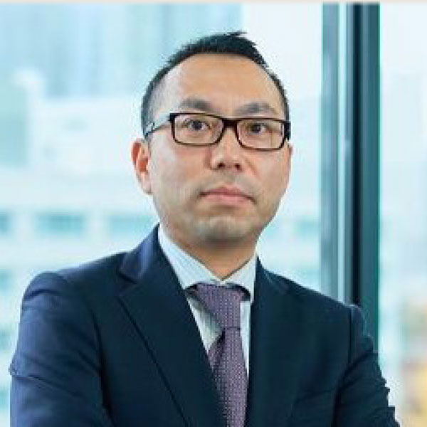
Hisashi Kanazashi
Director IT Div., METI
Bio:
He entered to the Ministry of International Trade and Industry in 1998. He was a visiting fellow at Stanford University and received his MBA from EDHEC Business School.
He has successively hold the positions at Industrial Revitalization Division, Economic and Industrial Policy Bereau and at Policy Planning and Coordination Division, Minister's Secretariat since 2009.
He also has experienced the positions of Director of Japan's Economic Revitalization Secretariat, Cabinet Sectetariat, as well as Deputy Commissioner of Los Angeles Office, Japan External Trade Organization, and Director of Industry Creation Policy Division, Economic and Industrial Policy Bureau, etc., since 2014. He has been on his current position since July 2022.
Abstract:
The environment surrounding the digital industry, digital infrastructure and the semiconductors they are based on is facing significant changes. These include the advance of digitalization due to COVID-19 responses, the moves toward carbon neutrality by 2050, tight supply/demand conditions of semiconductors worldwide, trade issues surrounding cutting-edge semiconductors and digital technologies, and economic security.
In this presentation, the strategy of Japan's semiconductor industry recognizing these changes, including enhancement of basic semiconductor production capacity, technology development for beyond 2nm next generation semiconductor will be presented.
Tetsuro Higashi
Chairman of the Board of Directors, Rapidus Corp
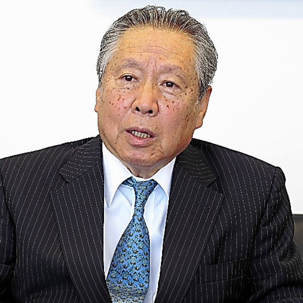
Tetsuro Higashi
Chairman of the Board of Directors, Rapidus Corp
Bio:
TETSURO HIGASHI is the first Chairman of the Board of Directors at Rapidus Corporation, a company that researches, develops, designs, manufactures, and sells advanced logic semiconductors, in August 2022.
Prior to this role, Higashi had held a series of executive roles at Tokyo Electron Limited from 1990 until 2019 when he resigned from his position at the company. After his experience as Vice President at the company’s Motorola Sales Department and the Diffusion Systems Department, and General Manager at the SPE 2 Division, he had joined the executive board as Corporate Director in 1990. Following that, he was appointed to President and CEO of the company starting from 1996 when he was 46 years old. He had become Chairman of the Board in 2003 and reappointed as President and CEO in a dual role in 2013. In 2016, he had was appointed Corporate Advisor and resigned from his position at the company in 2019.
Mr. Higashi holds senior positions at several organizations related to semiconductor and technology including Directors Emeritus of SEMI (Semiconductor Equipment and Materials International) since 2012, Advisor of SEAJ (Semiconductor Equipment Association of Japan) since 2016, and Chairperson of the Executive Board of TIA since 2017. In addition, he was appointed to Chairman of Leading-edge Semiconductor Technology Center (LSTC), an organization that conducts next-generation semiconductor research, in 2023.
Mr. Higashi was born on August 28, 1949, in Tokyo, Japan and received a B.A. (1973) in Social Science from International Christian University and a M.A. (1977) in Social Science from Tokyo Metropolitan University.
Abstract:
At first, talk about the historical change in the world of regional semiconductor market share and its meaning, and then raise the issue why leading-edge semiconductor technology becomes so critical and vital for national security and economy. Lastly overview the role and mission of “Rapidus” and “LSTC” which represent the Leading-edge Semiconductor Technology Center in Japan.
Frédéric Godemel
EVP & Power Systems and Services, Schneider Electric
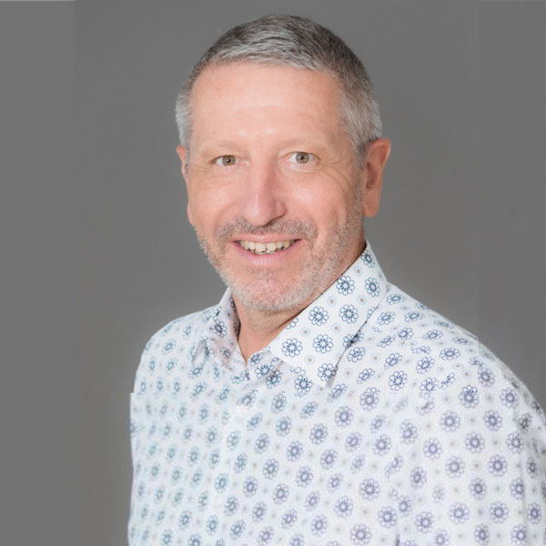
Frédéric Godemel
EVP & Power Systems and Services, Schneider Electric
Bio:
Frederic Godemel joined Schneider Electric in 1990. Since then, his career has developed mostly around the power business in both low and medium voltage. Frederic has held operational functions in France, China and more recently in Dubai, he is now back in France. He was appointed Executive VP for Global Field Services back in 2018, EVP for Power Systems in January 2019 and more recently in July 2020 Executive VP for Power Systems and Services. Frederic is participating in speaking and panel opportunities on behalf of Schneider Electric, the most recent were TAQA in Abu Dhabi, TSIA in Orlando, CERA Week Houston and Reuters London. Frederic graduated from the Ecole Centrale Nantes in electrical engineering and holds an MBA from ESSEC Business School.
Abstract:
A more electric and digital world, which we call Electricity 4.0, is key to addressing the climate and energy crises and unocking a sustainable and resilient future. Electricity is the most efficient energy and the best vector of decarbonization, and with digital innovation it unleashes huge potential to eliminate energy waste. Only by disrupting the way we manage energy can we deliver a net zero carbon world.
The semiconductor industry also has the responsibility to transform its energy use for a net-zero future. The good news is that semiconductor companies have made many commitments to decarbonize their operations, especially their fabs. But how are they delivering on their green promises?
Join this inspiring talk from energy and automation leader Schneider Electric to explore the value of digital energy technology and meaningful partnerships that help ensure a bright and sustainable future for semiconductor companies.
Agnieszka Thonet
Senior Director of Technology, HP

Agnieszka Thonet
Senior Director of Technology, HP
Bio:
Agnieszka has over 23 years of digital transformation and product innovation experience. Recognized as a thought leader in emerging technologies and trends, she has a strong track record of managing and aligning global high performance multicultural teams to deliver strategic value.
Over the past 16 years she has held multiple technical and management roles across HP businesses. As Senior Engineering Director, she drove the delivery of full stack software on devices and to Enterprise customers. As Head of Innovation Partnerships, she gathered and led cross-industry, multidisciplinary research experts to create open collaboration models that unleashed impactful innovation. Her breadth of knowledge ranges from electronics and communication systems to digital manufacturing and complex cyber-physical architectures.
Fluent in four languages, she holds a MSc in Communication Systems Engineering from the University of the Basque Country in Spain.
Pierre Barnabé
CEO, Soitec
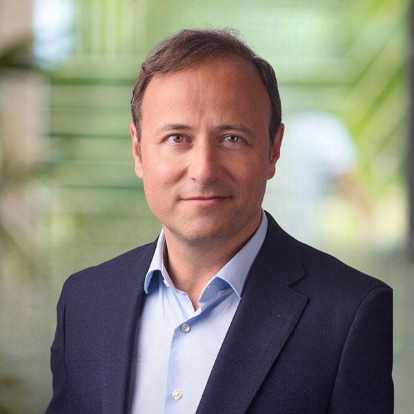
Pierre Barnabé
CEO, Soitec
Bio:
Pierre Barnabé was nominated as Soitec CEO in January 2022 and joined the company four months later.
He was previously Executive Vice-President in charge of Big Data & Cybersecurity at technology group Atos (2015-2021), where he also led the Public Sector & Defense division and manufacturing operations before serving as interim Group CEO in 2021.
Prior to its acquisition by Atos in 2014, Pierre Barnabé was Deputy CEO of Bull. He then served as Bull’s Chairman & CEO from 2015 to 2021, spearheading the company’s evolution into a global leader in cybersecurity services and supercomputing.
From 2011 to 2013, he was Managing Director of the Enterprise branch of SFR, the French telecoms operator, where he launched cloud computing and very high-speed broadband activities.
That followed a 13-year stint during which he held various positions at Alcatel and Alcatel-Lucent, first in sales and later as Chairman & Managing Director of Alcatel-Lucent France (formerly Alcatel CIT) and Group Deputy Managing Director for Human Resources and Transformation.
A graduate of the NEOMA Business School and Ecole Centrale in Paris, Pierre Barnabé began his career in 1994 in Silicon Valley, developing corporate venture capital and capital risk activities for Thales Group. He then moved to Thales headquarters in Paris, where he was in charge of strategy and acquisitions for the Communication and Command division.
A member of the board of the multinational market firm Ipsos, he also served as Chairman of the Board of ENSIMAG Grenoble, the prestigious Grande École specializing in computer science, applied mathematics and telecommunications (2016-2022) and on the board of France’s National Institute for Research in Digital Science and Technology (INRIA) from 2021 to 2022. Pierre Barnabé is a Knight of the French National Order of Merit.
Tim Archer
CEO, Lam Research
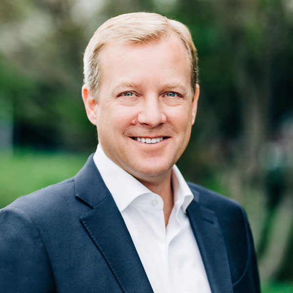
Tim Archer
CEO, Lam Research
Bio:
Timothy M. Archer is president and chief executive officer at Lam Research. During his tenure as CEO, he has driven revenue growth of more than 50%* and an EPS increase of more than 85%*. He joined the company in 2012 following its acquisition of Novellus Systems, Inc. (“Novellus”) when he began serving as Lam’s executive vice president and chief operating officer. He was later promoted to president and chief operating officer, and then president and chief executive officer in December 2018.
Tim currently serves on the International Board of Directors for SEMI, the global industry association representing the electronics manufacturing and design supply chain. From 2020 to 2022, he served as chairman of the board for the National Consortium for Graduate Engineering Degrees for Minorities (GEM): a nonprofit organization in the U.S. that is dedicated to increasing the participation of underrepresented groups in engineering and science at the master’s and doctoral levels.
Prior to joining Lam, Tim had an 18-year tenure at Novellus where he served as the company’s COO, and held other executive positions supporting worldwide sales, marketing, customer satisfaction, and product and business development. He began his career at Tektronix, Inc. in 1989, developing processes for high-speed bipolar integrated circuits.
Tim completed the Program for Management Development at the Harvard Graduate School of Business and earned his B.S. degree in applied physics from the California Institute of Technology.
*Calendar year 2018 compared to calendar year 2021
Abstract:
Increasing speed and scale to deliver on the future of specialty technologies.
Specialty technologies are ubiquitous – an essential connection between our physical and digital worlds. Poised to play an even bigger role in how we live and interact every day, it’s critical to accelerate device development and improve high volume manufacturing. However, as one of the most technically and geographically fragmented market segments, achieving greater speed and scale is challenging. It’s time to leverage the latest innovations including more advanced, application specific tools, virtual process development, and Equipment Intelligent® capabilities in the specialty technologies market to deliver on the future of a smaller, more connected world.
Serge Nicoleau
Group VP Technology, STMicroelectronics
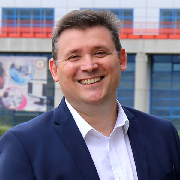
Serge Nicoleau
Group VP Technology, STMicroelectronics
Bio:
Since 2024, Serge Nicoleau is Group Vice-President Technology in charge of defining, implementing, and driving the R&D governance of Digital and BCD technologies of STMicroelectronics. He started his career in STMicroelectronics in 1998 in manufacturing management of the 200mm Crolles fab, nearby Grenoble. After various positions in manufacturing, process engineering, equipment engineering, he joined in 2004 the Crolles 300mm fab within the Crolles2 Alliance between STMicroelectronics, Motorola/Freescale and Philips/NXP. In 2007, he became Director of Industrial Technologies, before enlarging his responsibilities in 2012 as Deputy Director of the Operations of both Crolles 200 and 300 fabs.
This role included a specific responsibility for the industrial challenges of Automotive and IoT products in technologies ranging from 0.5μm down to 28nm critical dimensions with their multiple variants and options. In 2018, Serge Nicoleau is engaged into the new STMicroelectronics 300mm fab program in Agrate (Italy) to support Smart Power, Analog Mixed Signal and eNVM products. Then in 2020, he took the responsibility of the Technology & Design Platforms organization as General Manager. This organization is covering digital technologies, fast analog technologies, embedded memories, and optical sensors, with teams in France, in India, in United States which are addressing the digital products of STMicroelectronics.
Serge Nicoleau holds an Engineering Degree of the Ecole Polytechnique (Paris), a master’s degree in Theoretical Physics of the Ecole Normale Supérieure (Lyon) and a PhD in Particle Physics.
Sébastien Dauvé
Chief Executive Officer, CEA-Leti
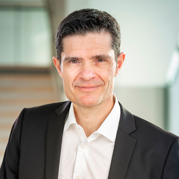
Sébastien Dauvé
Chief Executive Officer, CEA-Leti
Bio:
Sébastien Dauvé was named CEO of CEA-Leti effective on July 1, 2021, after more than twenty years of experience in microelectronics technologies and their applications, including clean mobility, medicine of the future, cybersecurity, and power electronics.
Sébastien Dauvé started his career at the French Armament Electronics Center, where he worked on developing synthetic-aperture radar. In 2003, he joined CEA-Leti as an industrial transfer manager and supervised several joint research laboratories, in particular with the multinational Michelin.
In 2007, Sébastien Dauvé became a laboratory manager, then head of an R&D department in the area of sensors applied to the Internet of things and electric mobility. During this time, he supported the dissemination of new technologies in industry, including the automotive industry (Renault), aeronautics, national defense (SAFRAN), and microchips with the industry leader Intel. He played an active role in the creation of start-ups in application fields ranging from health to infrastructure security, leading to dozens of new jobs. In 2016, he became Director of the CEA-Leti Systems Division.
From sensors to wireless communication, Sébastien Dauvé has played an active role in the digital transformation, focused on coupling energy frugality and performance. He has made cross-disciplinary approaches central to innovation by harnessing the expertise of talented teams with diverse backgrounds. Their goal is to provide technological tools for meeting the major societal challenges of the future.
Sébastien Dauvé is a graduate of the French Ecole Polytechnique and the National Higher French Institute of Aeronautics and Space (ISAE-SUPAERO).
Jean-René Lèquepeys
Deputy Director and Chief Technology Officer, CEA-Leti
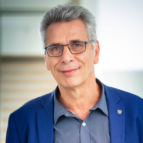
Jean-René Lèquepeys
Deputy Director and Chief Technology Officer, CEA-Leti
Bio:
Jean-René Lèquepeys received an engineering degree in 1983 from CentraleSupélec, a top French graduate engineering school at Paris-Saclay University, France. He taught physics during 2 years in Ouarzazate, Morocco.
He joined CEA, a French Research and Technology Office focusing on applied research, in Paris Saclay in 1985. He first worked at the laboratory of the Central Security Office, on the evaluation of means of detection and intrusion. Two years later, he was promoted head of this laboratory.
In 1993, he moved to Grenoble, France, and joined the System Division of CEA-Leti. He worked on different projects in the field of image processing and telecommunication technologies. In particular, he was responsible for the "Telecom, Communicating Objects and Smart Card" programs from 1999 to 2004.
In 2005, he took the responsibility of the Circuits Design Division at CEA-Leti (200 people). He launched new research activities at CEA such as a new laboratory in Aix-en-Provence, France, on the development of secured chips. In 2000, Jean-René Lèquepeys received the prestigious award from the french Société de l'Electricité, de l'Electronique et des technologies de l'information et de la communication (SEE) "Grand Prix de l'électronique Général Ferrié" for his work in the telecommunications field (he holds 15 patents).
In 2010, he launched a new division at CEA focusing on Electronic Architectures, Integrated Circuit Design and Embedded Software. He established the structure on two sites (Paris and Grenoble) and led the division twice in his career.
He rapidly got involved in the creation of the Silicon Components Division at CEA-Leti, and took the lead of it in 2011 managing 350 people. Division encompasses micro and nanoelectronics (SOI, nanodots, quantum, memories, 3D technologies, substrates), Micro Systems (sensor, actuator, radiofrequency components) and Power Components. He established the French Nano2022 Program for research funding in microelectronics.
In 2019, he was appointed Chief Technology Officer of CEA-Leti, overseeing Science, relations with the European Commission, Industrial Partnership and Strategic Program Management in the scope of the institute (2,000 people, ~€350m budget). He took the responsibility of the Microelectronic Program at CEA level, spearheading technological and upstream research in the field of semiconductor technologies. For the past 2 years, he has been strongly involved in the CEA-Leti Next Gen FD-SOI project in the frame of France2030 and has played a key role in European chips Act pilot line promoting FD-SOI and Gate All Around technologies.
Having dedicated his career to applied research, he is regularly invited as a keynote speaker in international semiconductor conferences.
Jean-René is also Vice President of ACSIEL, a professional trade union gathering industrial companies in the French electronic value chain, member of the Board of EPOSS, the European Technology Platform on Smart Systems Integration, a member of the Board of AENEAS, the Association for Europoean NanoElectronics Activities, and an expert consultant for the European Commission and French Research Agency
Michael Tchagaspanian
EVP Strategic Partnership, CEA-Leti
Michael Tchagaspanian
EVP Strategic Partnership, CEA-Leti
Sustainable Electronics
Léa Di Cioccio
Eco-Innovation Program Manager, CEA-Leti
Léa Di Cioccio
Eco-Innovation Program Manager, CEA-Leti
Léa Di Cioccio is Director of Research at CEA-Leti. She is currently in charge of the CEA-Leti Eco innovation program.
Since 1990, when she joined the organization, she has conducted research activities in materials, epitaxy, direct bonding, etc. in the fields of 3D integration and power components in the frame of collaborations with STmicrolectronics, SOITEC and in lots European projects. She is the author of more than 200 publications, 5 book chapters and 40 patents. Concerned by the socio-ecological transitions underway, she is working to introduce these new paradigms into the organization's research methodologies and strategy.
Laurent Pain
Sustainable Electronics Program Director, CEA-Leti
Laurent Pain
Sustainable Electronics Program Director, CEA-Leti
Bio:
Laurent Pain is graduated from the Ecole Nationale Supérieure de Physique de Grenoble in 1992. He received his Ph D after his work on DUV resists study. He joined CEA-Leti in 1996 to work on infra-red technology, and then came back to STmicroelectronics in 1999 working on 193nm and e-beam lithography technologies.
From 2008 to 2014, Laurent Pain leaded the lithography laboratory of the silicon technology division of CEA-Leti. He was also managing in parallel the industrial consortium IMAGINE dedicated to the development of multibeam lithography with MAPPER lithography BV.
Since July 2014, within the CEA-Leti Silicon Technology Division, he is now in charge of the business and the partnerships developments of the Silicon Technologies Platform Division.
Abstract:
The semiconductor industry underpins global digital transformation, with the ICT market expected to double by 2030 due to advances in AI, 5G, and cloud computing. A fundamental shift toward more resilient, sustainable, and circular manufacturing models is required to enable this growth. Key challenges include reducing water, gas, and metal consumption, minimizing PFAS dependence, and improving effluent circularity.
Attendees will hear how CEA-Leti’s comprehensive sustainability roadmap spanning the entire semiconductor value chain will integrate process innovation with system-level optimization to drive measurable environmental impact reduction. The SubFAB Labs initiative, developed in collaboration with International SubFAB Research Labs (ISRL), is a central pillar of the roadmap. This four-year program, which can be extended, will evaluate the subfab environment, from process to final waste treatment by improving material use, abatement strategy and global effluent? circularity. The aim is to reduce costs and global environmental impact.
Jérôme Daviot
R&D and Application Director, Deputy General manager, Technic
Jérôme Daviot
R&D and Application Director, Deputy General manager, Technic
Bio:
After participating and leading chemical design programs throughout various industrial ventures, ranging from a Ph.D. on hydroxylamine cleaning to Cu PCMP with EKC Technology, and further enriched by assignments at prominent European RTOs (LETi, IMEC), he transitioned to the role of R&D director for the Strip/Etch/Clean group at Technic. Over the past 14 years, his team's mandate has been to tackle, refine, and optimize innovative wet processes that could effectively address performance, sustainability, and HSE concerns. Utilizing Technic's growing reputation for addressing industrial issues and wet process changes with a holistic approach, in tandem with chip manufacturers' ESG initiatives, allow to accelerate evaluations and acceptance of innovative eco-designed blends. Recent initiatives such as the CLEAN consortium (LETI/STM/Technic) represent significant contributions to fostering a gradual shift in mindset and showing that designing wet processes in a more systemic eco-friendly way can also offer valuable cost of ownership in the long run.
Slava Libman
CEO, FTD Solutions
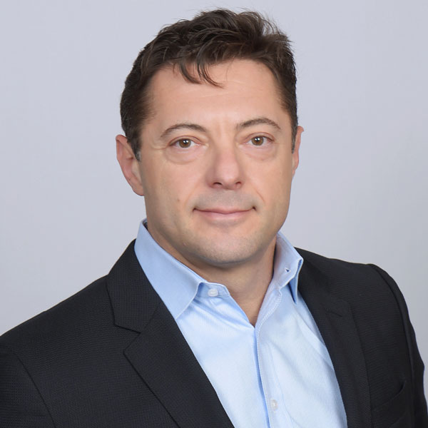
Slava Libman
CEO, FTD Solutions
Bio:
Dr. Slava Libman is a thought leader, passionately driving innovation in sustainability with over 25 years of experience in water technology. As a Co-Founder and CEO of FTD Solutions, he leads an early-stage company dedicated to helping complex industrial facilities tackle sustainability challenges through the use of advanced digital twins. These tools empower organizations to visualize their data, diagnose issues, and make data-driven decisions to optimize performance.
Under Dr. Libman's leadership, FTD Solutions has assembled a highly skilled team that has collaborated with numerous global corporations to solve countless challenges. Their combined efforts have resulted in savings of hundreds of millions of dollars, risk mitigation, and an impressive water conservation record reaching billions of gallons. Slava's unwavering commitment to sustainable practices and technological advancements positions him as a thought leader in the industry.
Slava champions environmental and operational sustainability in the semiconductors via industry wide activities. He is a co-chair of Environmental Sustainability forum of IRDS, Yield Enhancement forum of IRDS, as well as SEMI Standards Water Reuse Task Force. Slava is a lead moderator of the International UPM Conference driving innovation in semiconductor facilities.
Isabelle Servin
Sustainability Advisor and Eco-Design Engineer, CEA-Leti
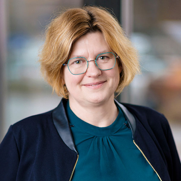
Isabelle Servin
Sustainability Advisor and Eco-Design Engineer, CEA-Leti
Bio:
Isabelle SERVIN is a research scientist at CEA-Leti, Grenoble (France). Since 2022, she has joined the eco-innovation program, as sustainability advisor for Technological Silicon Platform. She evaluates the environnemental impacts of processes in clean room through The Life Cycle Assessment (LCA) methodology for IC industry. She has 20 years of experience in the development of lithography processes for microelectronics, both in industry and R&D. She received her PhD on polymer chemistry from University Pierre & Marie Curie (Paris, France) in 1998.
Abstract:
In semiconductor industry, energy efficiency and water management are crucial to reduce the environmental impacts of chips manufacturing.
CEA-Leti will propose ways to improvement energy efficiency both to infrastructure and production equipment.
Additionally, techniques such as water reuse and adoption of advanced technologies for water treatment and purification are currently implemented to reduce water usage in cleanrooms, contributing thus to sustainable management of resources.
Joao Carlos Lopes Barbosa
Ph.D. Student, CEA-Leti
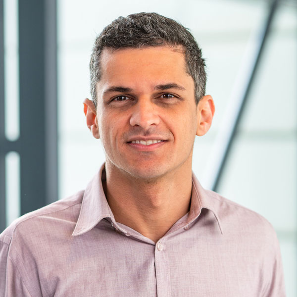
Joao Carlos Lopes Barbosa
Ph.D. Student, CEA-Leti
Bio:
I hold a master degree in sustainable industrial engineering (Grenoble-INP) and am a PhD student at CEA-Leti since Decmbre 2021. In my previous experiences, I conducted a comparative study of life cycle analyses of high quality papers produced with different types of fibers. My thesis at CEA-Leti aims to develop a tool to anticipate the environmental impacts of large-scale semiconductor products on the industry during the development phases using data collected in the research environment.
Abstract:
Semiconductor production requires strict control of the production environment to ensure product quality. The cleanroom must maintain a very low level of airborne particles, controlled temperature and humidity, and a slight overpressure. Large amounts of ressources such as water and electricity are required to maintain these conditions. Therefore, a significant portion of the environmental impacts in the semiconductor industry are due to the stringent requirements of cleanrooms.
A life cycle assessment war performed in the CEA-Leti clean room to evaluate th environmental impacts resulting from the requirements of semiconductor production. The results allow to identify the most important sources of impact and to stimulate a critical analysis of improvement points.
Yannick Rivoira
Sustainability Engineer, CEA-Leti
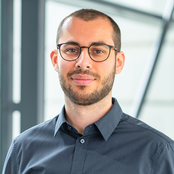
Yannick Rivoira
Sustainability Engineer, CEA-Leti
Bio:
Yannick Rivoira is a sustainability engineer at CEA-Leti since 2022. He is especially involved in environmental impacts assessments for microelectronics industry. This imply methodological development, data collection and comprehension at process and fab level as well as understanding the environmental issues and reglementations. He is specifically in charge of the Sustainability work package for the european project FAMES.
Abstract:
Microelectronics is a high-precision industry that is rapidly evolving. Better understanding its environmental implications and making this industry more sustainable is a complex challenge. This is why, inside the FAMES european project, a methodology and a software for assessing environmental impacts are being developed. The main objective is to add an Environmental criterion to the traditional Power-Performance-Area-Cost (PPAC) optimisation by taking into account environmental impacts from design to chip manufacturing.
Sandrine Catrou
VP Marketing and Strategic Partnership, CEA-Leti
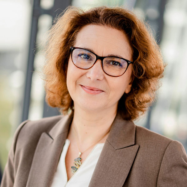
Sandrine Catrou
VP Marketing and Strategic Partnership, CEA-Leti
Bio:
Sandrine Catrou holds an Electrical Engineering degree and a Master degree in microelectronics both obtained in Bordeaux, France, in 1991.
She spent her first 15 years in chips design, alternatively at European Silicon Structures, Rousset, France, ATMEL Corporation, and STMicroelectronics, Grenoble, France.
In 2011, she joined CEA Technology Transfer Office in Grenoble, France, supervising market studies in microelectronics. She got involved in the launch of a dozen CEA deeptech startups in France.
In 2015, she joined CEA-Leti CTO office as Strategic Marketing Manager to provide semiconductor market insights. In particular, she got involved in major national strategic investment plans in microelectronics.
In 2020, Sandrine started developing CEA-Leti international industrial partnerships with semiconductor industrial leaders. She got involved in the High Level Forum to foster international collaborations between innovative clusters. She also got involved in the development of technological collaborations between Grenoble Silicon Valley and the K-Belt.
Abstract:
Insights into the semiconductor and electronics industries will concentrate on the latest market and technology trends. This analysis will explore design opportunities unlocked by innovative semiconductor technologies, with a special emphasis on FD-SOI technology, covering its current adoption status and market outlook. Driven by the promising advantages of FD-SOI transistors—ideally suited for a wide range of next-generation electronic applications—a new industrial ecosystem has emerged, fostering increased design wins and accelerating technology adoption.
Etienne Lees-Perasso
LCA & Ecodesign Consultant, TIDE
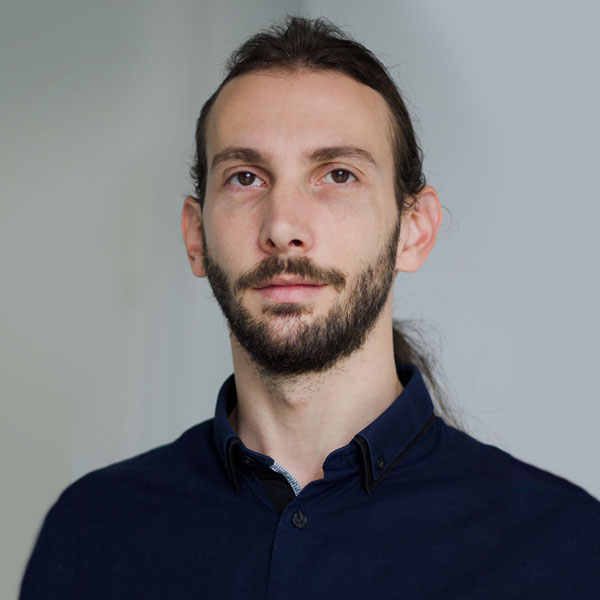
Etienne Lees-Perasso
LCA & Ecodesign Consultant, TIDE
Bio:
Etienne holds a Grenoble INP Master’s degree in industrial engineering specialized in supply chain and ecodesign.
He conducts LCA studies within the digital, electric and electronic, transport and building sectors following different objectives: research, environmental declarations (PEP ecopassport, FDES, EPD), ecodesign projects and decision-making support. He regularly assists firms and authorities on the methodological and technical aspects through trainings: LCA, environmental communication, etc.
Etienne also develops LCA data and databases, such as the EIME and Negaoctet databases.
Abstract:
The last decade saw the acceleration of new technologies adoption, shaping the digital landscape in terms of speed, quality and connectivity for multimedia contents and communication tools. While many activities have been able to benefit from the numerous innovations (4.0 industry, e-commerce, telecommunications, etc.) to develop, this growth has always been coupled with a significant increase of pressures on the environment and natural resources.
This study is part of an analysis process, but also of a prospection process related to digital technologies future. It covers the whole digital perimeter, from the network installations to terminals and considering the network, equipment and datacenters impacts.
Specifically, it consists in an evaluation of France digital technologies impacts with the Life Cycle Assessment (LCA) methodology.
It covers the 3 tiers of digital technologies: user terminals, networks and datacenters, and calculates a panel of 12 impact indicators, including climate change, natural resource consumption or particulate matter.
Results are presented a the France-wide scale, per inhabitant, and are detailed under several levels of analysis in order to get a more acute interpretation, and a better comprehension of direct environmental stakes related to digital technologies in France.
Limitations are discussed in order to highlight improvement opportunities.
Valentin Landmann
Head of Ecosystems Development, STMicroelectronics
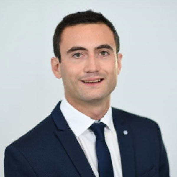
Valentin Landmann
Head of Ecosystems Development, STMicroelectronics
Bio:
Double master degree in France and Germany at Arts et Métiers (ENSAM) and Karlsruhe Institute of Technology (KIT)
Diverse functions within the Tier-1 automotive manufacturer, ZF Group : Trainee Program (Friedrichshafen, Germany), project management in the field of Quality (Saarbrücken, Germany), European external affairs (Brussels, Belgium)
Recently joined STMicrolectronics SAS as Head of Ecosystems Development (Paris, France)
Abstract:
Many different environmental impacts arise from electronics, and the handling of electronic waste (E-waste) is rising quickly to the top of the agenda. E-waste is a significant issue for Europe: improving its management is an explicit goal of the Green Deal objectives and the Circular Economy Action Plan. However, due to the requirement to involve the whole value chain, from raw material suppliers to consumers, the complex material background and supply chain, as well as the multitude of competing interests, achieving circularity in the electronics industry is challenging.
This project main goal is to reduce E-waste in Europe by managing existing E-waste, developing new tools to extend electronic devices lifetime and increasing recyclability of E-waste. Finally, the EECONE project will focus on deployment of new best practices at European level and on the development of a new strong ecosystem in this domain.
Patrick Blouet
Sustainability Advisor
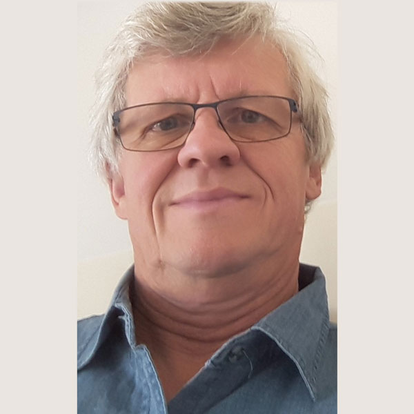
Patrick Blouet
Sustainability Advisor
Bio:
Patrick Blouet is an electronic and computer science engineer. He is now newly retired but spent more than 40 years in the electronic and semiconductor industry. He had different responsibilities in developing hard real-time systems, image processing systems, in charge of architecture of mobile products in STMicroelectronics and other large and small companies. He spent also several years in the European and public affairs team in STMicroelectronics where he had opportunity to build large European project around semiconductor technologies. He was also chairman of the Green ECS working in charge of defining what to do to make European electronic greener. This led to the creation of the EECONE project with objective to reduce electronic waste. He is interested in environmental and climate issues for more than 30 years and also member of the Shift project.
Abstract:
Many different environmental impacts arise from electronics, and the handling of electronic waste (E-waste) is rising quickly to the top of the agenda. E-waste is a significant issue for Europe: improving its management is an explicit goal of the Green Deal objectives and the Circular Economy Action Plan. However, due to the requirement to involve the whole value chain, from raw material suppliers to consumers, the complex material background and supply chain, as well as the multitude of competing interests, achieving circularity in the electronics industry is challenging.
This project main goal is to reduce E-waste in Europe by managing existing E-waste, developing new tools to extend electronic devices lifetime and increasing recyclability of E-waste. Finally, the EECONE project will focus on deployment of new best practices at European level and on the development of a new strong ecosystem in this domain.
Laura Vauche
Sustainability Advisor & Ecodesign Engineer, CEA-Leti
Laura Vauche
Sustainability Advisor & Ecodesign Engineer, CEA-Leti
Bio:
Laura VAUCHE, PhD is implementing Life Cycle Assessment (LCA), eco-design and eco-innovation at the Silicon Components Division (DCOS) at CEA-LETI since 2021. She obtained a Master’s degree in Chemistry in 2011 from Chimie ParisTech PSL and was awarded a PhD in Engineering Science: Micro and Nano-Electronics in 2015 from Aix-Marseille University. Her previous work includes process development, process integration, characterization and optimization of materials, semiconductors and devices for energy applications such as solar cells (thin films, silicon and multi-junction) and GaN power electronics.
Abstract:
Wide Band Gap (WBG) semiconductors have the potential to provide significant improvements in energy efficiency over conventional silicon (Si) semiconductors. While the potential for energy efficiency gains is widely researched, the the energy use during manufacturing processes and other environmental impacts remains insufficiently studied. No or sparse LCA data is available for the two currently most widespread WBG semiconductors materials are gallium nitride (GaN or GaN/Si) and silicon carbide (SiC). This paper, for the first time, presents a cradle to gate life cycle assessment for a GaN power device,The results identify environmental hotspots associated with different materials and processes.
Josua Guerid
Research Engineer – Eco-innovation & LCA, CEA-Leti
Josua Guerid
Research Engineer – Eco-innovation & LCA, CEA-Leti
Bio:
Mr. Josua Guérid is a Life Cycle Assessment (LCA) and Eco-Design specialist at CEA-Leti, the French RTO for microelectronics and digital technologies. He is an engineer from Ecole Centrale de Lille (2015) and also graduated from Arts & Métiers ParisTech on Change Management and Sustainable Innovation (2020). His fields of expertise are the assessment of environmental impacts of ICT and sustainable ICT.
References :
J. Guérid, J.-B. Doré, J. Reverdy, B. Reig, A. Clemente, and L. D. Cioccio, ‘Toward Eco-Design of a 5G mmWave Transmitarray Antenna Based on Life Cycle Assessment’, p. 6, 2022.
Abstract :
5G is seen as one technology enabler to support the expected exponential internet data-traffic growth while the environmental impacts of Information and Communication Technologies (ICT) are growing. Base stations are estimated to represent the main contributor to mobile internet access network carbon footprint. In this work, life cycle assessment (LCA) of two different technology of 26 GHz transmitarray antenna are compared. One technology demonstrates a drastic reduction, showing how environmental performance can be a key factor for the choice of technology.
Léa Roulleau
Sustainability Engineer, CEA-Leti
Léa Roulleau
Sustainability Engineer, CEA-Leti
Bio:
Léa is graduated from INSA Lyon (2020). She worked two years as LCA consultant-engineer at RDC Environment (Bruxelles). She works since April 2022 at CEA-Leti as LCA engineer-searcher.
Abstract:
Life cycle assessment of electronic components will be presented. The goal of theses studies is to quantify the environmental impacts, identify the main contributors, and find ways to reduce the environmental impacts. Theses studies focuses on fabrication step and relies on CEA-Leti flow definition and CEA-Leti cleanroom consumption and emissions.
Nicolas Leterrier
External partnerships leader, Schneider Electric
Nicolas Leterrier
External partnerships leader, Schneider Electric
Bio:
Nicolas Leterrier joined Schneider Electric in 2011. He held several positions in Schneider Electric in the field of technology & innovation as well as global labs VP. He is now working on external partnerships for semi conductor segment. Nicolas began his career in Paris working for Gaz de France and GFInformatique. In 1991, he joined ST Microelectronics as a software development engineer. After working in the US for data storage business development, he became in 1999 manager of an application development group covering the field of Telecommunications, Automotive and computer peripherals. He was nominated as SW development director for advanced multimedia product line in STMicroelectronics called Nomadik architecture. He managed teams in India and China in the scope of a software platform development. He worked to establish strategic partnership with major mobile phone providers. He joined KIS a French SME involved in the photo finishing business, to manage the R&D department. From 2006 to 2011, Nicolas Leterrier was the general manager of Minalogic, the global competitive cluster (Pôle de compétitivité) located in Grenoble, France. This cluster is actively working in the field of micro-nano technologies as well as embedded software to build collaborative projects between actors from industry, universities and public research centers. Initiated several agreements at European level with Germany and The Netherlands in the semiconductor field. Nicolas is graduated with a master of sciences of the Paris XI Orsay University and an engineering diploma from Ecole des Techniques du Génie Logiciel (software engineering).
Nicolas is passionate about resources efficiency in the field of energy, water and sustainable development. Initiated several initiatives on carbon footprint measure, understanding & reduction plus renewable integration to decrease carbon footprint and resources waste.
Abstract:
Sustainability is at the core of the century challenges. I'll describe in details the Sustainability Climate Consortium initiative from SEMI association gathering all the value chain of semiconductor industry. From materials providers, equipment manufacturer, chips engineering, semicon foundries as well as wemi conductors manufacturers and bis uders as web giant. This iniitiative is aiming on all scopes to address in a coherent maneer the carbon accounting, meaurement criterias, assessment and validation of carbon footprint. Also the solutions towards carbon footprint reduction on scopes 1, 2 & 3 plus ambition setting across the industry.
On behalf of Schneider Electric, I will explain our net 0 project and how our company is currently addressing the carbon footprint reduction across all its value & supply chain. How we measure ous emissions scopes and how we partner with our suppliers to reduce our carbon foortprint. In the same spirit, we aim at reducing our scope 2 by integrating more renewables in our different sites across the globe but also at the same time lowering the demand side in reducing energy consuption.
Rémi Bastien
CEO, NextMove
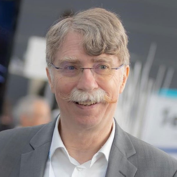
Rémi Bastien
CEO, NextMove
Bio:
Remi BASTIEN received his Engineer Diploma from ECAM in 1980. He joined RENAULT group in 1982, and after different responsibilities, he was Vice President for Research and Innovation for RENAULT Group (2009-15), before becoming Global Director for Autonomous Driving Prospective at the Renault/Nissan Alliance (2015-16) and finally Vice President, Automobile Prospective for RENAULT Group till 2021. He is honorary chairman of NEXT MOVE (French cluster dedicated to mobility), CTO of FISITA and member of the Shift Project (think tank for sustainable economy). He was member of the EUCAR council (former chairman in 2012) and Chairman of VEDECOM (French cooperative research institute) from 2017 to 2020, and Director of the program “Power Electronics” for French Automotive Industry and French Electronic Industry from 2020 to end of 2021. He is the co-author with Luc JULIA of the book “On va droit dans le mur?”.
Abstract:
Electronics plays a growing role in the automobile, for supporting electrification, safe driving or confort.
this ues will be crucial for moving towards carbon neutrality. On the other hand, the growing size of the software (embedded and off board) requires more powerful chips and increase the energy needs, and therfore higher CO2 consequences. In addition, these components will use some rare raw materials and to have a sustainable industry, it is mandatory to move to circular economy. All of these factors will lead to new designs called ecodesign were the way to optimize the systems must consider the full life cycle, and especially the way to disassemble the different ECUs and to get back the rare materials for recycling them in future systems.
Nadia Wetzler
Sr. Director – Global Legal Services, Applied Materials

Nadia Wetzler
Sr. Director – Global Legal Services, Applied Materials
Bio:
Nadia Wetzler is a Sr. Director in the Applied Materials law department. In that role, Nadia is responsible for providing legal counseling to the company on environmental, health and safety and sustainability matters. Nadia works closely with Chris Librie, Applied Materials director of ESG, corporate sustainability and reporting, on accelerating the company's environmental, social and governance programs. In addition, Nadia provides legal support to the company's Supply Chain Certification for Environmental and Social Sustainability (SuCCESS2030), the company's 10-year roadmap for creating a more sustainable supply chain. She has also partnered with a variety of Applied Materials business units on supplier and customer commercial matters. Nadia has been with Applied Materials since 2004.
Prior to Applied Materials, Nadia was an associate at Bingham McCutchen LLP, where she represented corporate clients on a number of environmental legal matters. Previously, she served as regional counsel at the US EPA Region 9 offices in San Francisco, California.
Nadia holds a JD from the University of California, Berkeley, School of Law and an undergraduate degree in economics and international studies from Yale University.
Yasumitsu Orii
Senior Managing Executive Officer, Rapidus Corporation
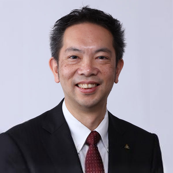
Yasumitsu Orii
Senior Managing Executive Officer, Rapidus Corporation
Bio:
Dr. Yasumitsu Orii joined IBM Japan in 1986 and was a leading expert on Flip Chip organic packages, which had contributed to the performance improvements and miniaturization of such products as servers, laptop computers, and HDDs. The packaging technology is becoming more important for next generation server products as Moore’s Law reaches its limits. His flip chip expertise extended into many related areas. Initially, he was a pioneer of flip chip on FPC (Flexible Printed Circuit) for HDDs, which allowed the read/write amplifier ICs to be mounted on the suspension and much closer to the GMR head. Later, he developed the C2 (Chip Connection) technology that supported low-cost 50-μm-pitch flip chip bonding for the commodity consumer electronics market and it was licensed to a company in Taiwan. At IBM Research Tokyo, he was leading the next generation flip chip organic package, 3D-IC projects and Neuromorphic Computing for IBM Servers and creating new technologies under a Joint Development Program involving many leading Japanese materials companies. He left IBM in 2014 and joined NAGASE & CO., LTD. He established “New Value Creation Office” under the direct control of the president and launched the material informatics software as a service in 2020. He left NAGASE and he joined Rapidus Corporation in 2022/Dec. Now he is the senior managing executive officer to lead the 3D Assembly Division.
Chris Bailey
Vice President Emerging Technologies, Edwards
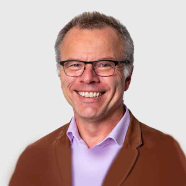
Chris Bailey
Vice President Emerging Technologies, Edwards
Bio:
Chris Bailey has been Vice President, Emerging Technologies at Edwards since 2017 with responsibility for developing technologies that increase the sustainability of semiconductor manufacturing processes. Examples include developing alternative vacuum and abatement system architectures that reduce energy consumption and footprint and also technologies for recovering and recycling process materials from the waste stream.
Chris Bailey joined Edwards in 1990 and has developed many vacuum pumps and abatement systems for the whole range of semiconductor process applications. Examples include Edwards El-JV Zenith for the El-JV Lithography application and Edwards Regis that extends the life of the vacuum system for a range of challenging vacuum processes.
Abstract:
With the development of IC manufacturing and the scarcity of resources and energy, sustainability is the key capability for industry resilience. Edwards, the enabler of low carbon manufacturing, collaborates with the industry for IC scaling and green transformation through our environmental innovation from the most advanced El-JV to the widely installed pumps and abatement.
Edwards will share global trend on sustainability, how we make EUV, CVD & etching processes greener through reducing, reusing & recycling to lower GHG, carbon emission & energy consumption without compromising uptime & safety.
- Global trend on Sustainability (net zero & SBTi) and government regulation (ex. US, Europe, Taiwan) Edwards' Innovation on green manufacturing — Lowering GHG & carbon emission
- EUV: Methodology of electro membrane hydrogen purification with fab data (recovery rate, purity, energy required & process transparency. ex, saving 73% of the energy usage v.s. the current practice)
- CVD: Lower NOX reduction
- Etch: Noble Gas (Krypton and Xenon) recycling
- The carbon footprint & cost (ex. carbon fee, carbon credit,..) saved and future opportunity
Yasutoshi Okuno
SCREEN
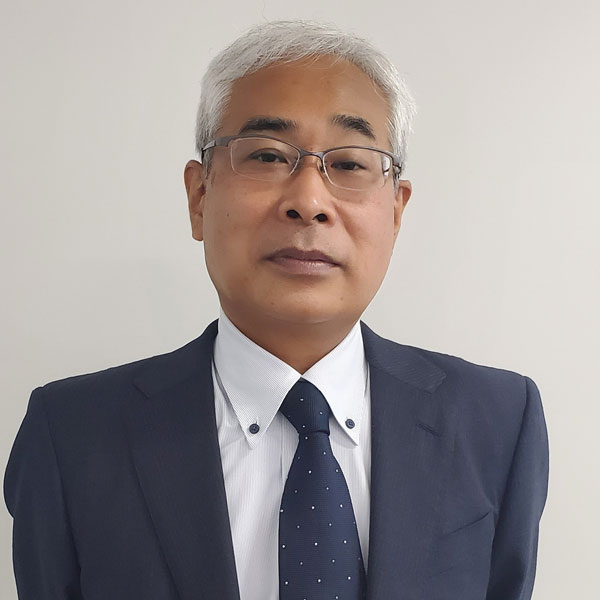
Yasutoshi Okuno
SCREEN
Bio:
Dr. Yasutoshi Okuno is a corporate officer and vice president of Technology Strategy at SCREEN Semiconductor Solutions Co., Ltd., a leading supplier of semiconductor equipment and solutions, especially for surface cleaning and wet treatment of wafers. He started his career as a member of the technical staff at Texas Instruments Inc., where he worked on memory and logic devices, and joint-development projects for DRAM with Hitachi and Mitsubishi. In 2010, he moved to TSMC as a department manager of the exploratory research program, where he engaged in advanced transistor research and development. In 2019, he joined SCREEN Semiconductor Solutions Co., Ltd. as a senior technical executive, and became a corporate officer and vice president of Technology Strategy in 2021.
James Newton
VP Business Development, Altyor Group
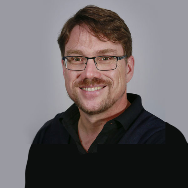
James Newton
VP Business Development, Altyor Group
Bio:
James’ pragmatic mindset, attuned to seeking out and applying new technologies where they bring their full potential and value, combined with his insatiable appetite for innovation means he has spent most of his professional life marketing cutting-edge solutions to large and small corporations in a wide array of industries.
From geographic information systems to AI-enabled IoT sensor development, his keenness to ever expand his scope of experience and tie together unrelated concepts to generate relevance and value in solving real-life issues has been blatant in his 25-year track record in developing and implementing solutions for companies such as Airbus, GrDF, Paprec, Société Générale, Suez, Total Energies and innumerable SMBs and start-ups.
As VP in charge of Business Development within Altyor Group, his focus is now on ensuring environmental transition through sustainable design, development, manufacturing and recycling of technological hardware in all fields where technology is relevant to improving our lives.
Anders S.G. Andrae
Assistant Chief Expert of Environmental Protection Technology, Huawei
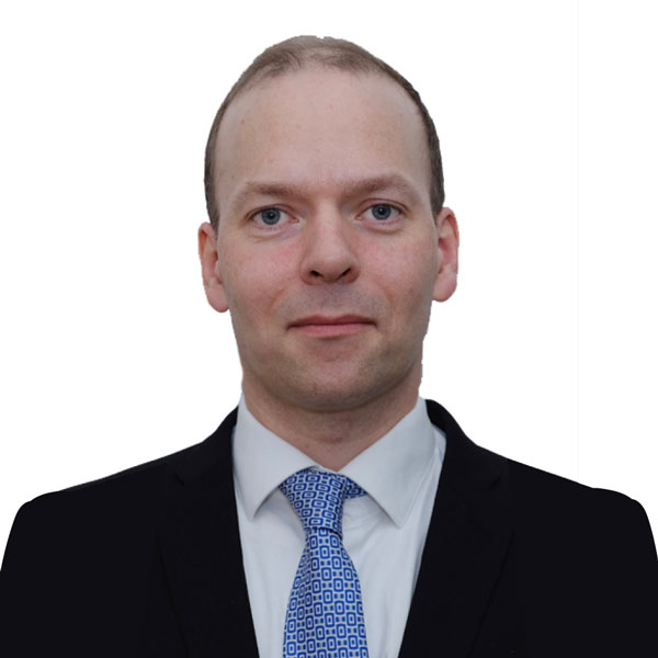
Anders S.G. Andrae
Assistant Chief Expert of Environmental Protection Technology, Huawei
Bio:
Dr. Anders S.G. Andrae received the Ph.D. degree in electronics production (microsystems packaging) from Chalmers University of Technology, Gothenburg, Sweden, in 2005.
He worked for Ericsson with Life Cycle Assessment (LCA) between 1997 and 2001. Between 2006 and 2008 he carried out post–doctoral studies at the National Institute of Advanced Industrial Science and Technology (AIST), Tsukuba, Japan.
His speciality is the application of sustainability assessment methodologies to ICT products, networks, services, systems and solutions from cradle–to–grave. He works on many topics in European Telecommunications Standards Institute’s (ETSI), International Telecommunication Union (ITU-T) and the International Electrical Commission (IEC) e.g. Product Circularity Scoring, LCA methods for IC modelling, reuse/replace trade-off and avoided emissions.
Since 2009 Dr. Andrae has been the Rapporteur and Editor of several ETSI and ITU-T Standards and Technical Reports about LCA and Circular Economy.
His current research interest is development and application of LCA to ICT to better understand footprint evolution, trade-offs, supply chains and business models as far as: data management, waste minimization, and green indicators. In ETSI standardization he helps define new LCA methodologies for ICT consumer and network infrastructure goods as well as product information formats.
He has previously published three books and 40 peer–reviewed journal papers.
Since 2008 Dr. Andrae has been with Huawei Technologies in Sweden now as Assistant Chief Expert of Environmental Protection Technology.
Vincent Semetey
Director of Research, CNRS & Head of the Chair, Chimie ParisTech - PSL
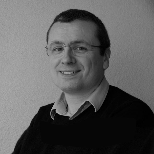
Vincent Semetey
Director of Research, CNRS & Head of the Chair, Chimie ParisTech - PSL
Bio:
Vincent SEMETEY received his PhD in chemistry from University of Strasbourg in 2002. He joined CNRS in 2005 at Institut Curie and moved to Chimie ParisTech - PSL in 2015. He has 20 years of experience in material sciences and more particularly recycling of metals and plastics. Since 2017, he is in charge of the Chair Urban Mines, a research and education program dedicated to circular economy and recycling of e-waste supported by ecosytem.
Martine Druges
ESH Director, STMicrolectronics

Martine Druges
ESH Director, STMicrolectronics
Bio:
Martine Druges is the ESH director of STmicrolectronics, She is an Experienced Manager with a demonstrated history of working in the semiconductors industry. Strong business development professional skilled in Projects Management including Fab 300mm Engineering & Fab Revamping, Process & Equipment Engineering, Facilities and HSE.
Quantum Computing
Jean-Charles Barbé
Quantum program scientific director, CEA-Leti
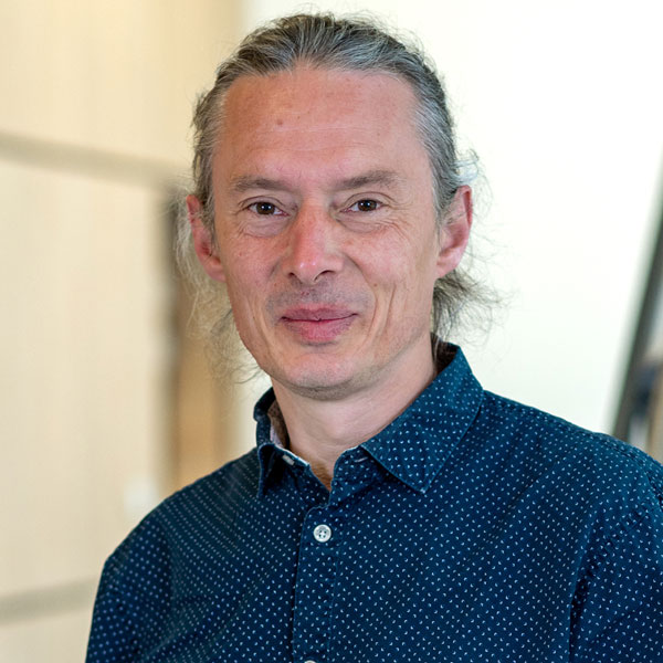
Jean-Charles Barbé
Quantum program scientific director, CEA-Leti
Bio:
Dr. Barbé received the M.Sc. and Ph.D. degrees from Ecole Polytechique de Grenoble respectively in 1997 and 2000. From 2010 to 2017, he managed the Simulation and Compact Modeling group. In this role, he leads Leti’s activities in modeling and simulation ranging from atomistic simulation to compact modeling for SPICE simulation. Until 2022, he was the scientific director of the Silicon components Division. He is now the Scientific Director of Leti’s Quantum Grand Program.
Dr Barbé was active contributor to the Simulation and Modeling Working Group at ITRS/IRDS and is member of the Technical Program Committee of the SISPAD conference. He has authored or coauthored about 80 papers in the fields of Nanoelectronics from material engineering to Devices physics and modeling. He owns more than 30 patents related to these fields.
Corinne Legalland
Quantum Program Director, CEA-Leti
Corinne Legalland
Quantum Program Director, CEA-Leti
Bio:
Corinne Legalland received the engineering degree from INP-Toulouse in 1995. From 2002 to 2011, she managed several technical teams (process engineering, parametric test, defect density) at Altis Semiconductor (now XFab France at Corbeil Essonnes – France). In 2012, she joined CEA-Leti as Silicon Technologies Department deputy manager, in charge of clean rooms operations (8000m2 clean rooms, serving 250 projects 200 and 300 mm, delivering 100 wafer lots per week). In 2018, she became key account manager for a major CEA-Leti industrial partner, managing a technical program of more than 100py per year covering Image sensors, nonvolatile memories, RF components, photonic and 3D technologies. Today, she is charge of quantum program direction at CEA-Leti, together with Jean-Charles Barbé.
Silvano De Franceschi
Research Director and CEA Senior Fellow, CEA-IRIG
Silvano De Franceschi
Research Director and CEA Senior Fellow, CEA-IRIG
Bio:
Silvano De Franceschi is an expert in quantum nanoelectronics and experimental mesoscopic physics. He received his PhD in 1999 at the Scuola Normale Superiore of Pisa and, he currently works as research director at the Interdisciplinary Research Institute of Grenoble (IRIG). In 2005 he was awarded the Nicholas Kurti European Prize for his achievements in the field of quantum transport and, in particular, his works on the Kondo effect in quantum dots and on hybrid normal/superconductor nanostructures. His current research activity focuses on the development of silicon-based devices for quantum information processing. He is co-leading the Grenoble Quantum Silicon Group (http://quantumsilicon-grenoble.eu) and he is CEA Senior Fellow for the field of quantum technologies.
Abstract:
Semiconductors and the ability to process them to the ultimate size are the cornerstone of nano- and optoelectronics.
How will semiconductor materials play a key role in the development of future quantum computers? In fact, semiconductor technology can provide not only the classical control hardware but also the quantum processor itself.
After a brief review of the different ways in which quantum information can be encoded and processed, I will highlight some of the scientific and technological prospects and challenges. In particular, I will focus on semiconductor spin qubits and present the latest results obtained by our team in Grenoble.
Maud Vinet
CEO, Siquance
Maud Vinet
CEO, Siquance
Bio:
Since 2022, Maud Vinet is CEO of Siquance who aims at developing and commercializing quantum computers based on silicon.
Previously she led the quantum computing program in Leti with the objective
of building a large scale quantum computer based on silicon VLSI technology.
She defended a PhD of Physics from University of Grenoble Alps and was hired Leti in 2001 as a CMOS integration and device engineer. From 2009 to 2013, she spent 4 years in Albany (NY, US) to develop Fully Depleted SOI within IBM Alliance together with STMicroelectronics. In 2015, she spent 6 month with Globalfoundries in Malta, NY to launch 22FDX program.
From 2013 to 2018, she managed the Advanced CMOS integration team activities in Leti. In 2019, she was appointed project leader for the quantum computing program in Leti.
Maud Vinet authored or co-authored about 300 papers, she owns more than 70 patents related to nanotechnology and her Google h-index is 52 with more than 11000 citations.
Abstract:
Siquance is a start up which span off from CEA and CNRS in 2022 to develop and commercialize universal quantum computing solutions based on CMOS technologies
Sillicon spin-qubits have demonstrated promising properties at the individual level, such as record spin lifetime and high-fidelity gates, and they derive directly from the transistor. With this in mind, they have potential to alleviate three bottlenecks of current prototypes to scale up. First, millions of them can be fitted in a square cm leveraging advanced CMOS technologies, second they can be monolithically integrated with the electronics that enable their fast and individual control, and finally they allow designing cost effective quantum computer for a pervasive use in the industry. Currently silicon spin qubits technologies are at the stage where they are facing the dilemma of the semiconductor industry, a highly structured industry with seamless processes from proof of concept to products that demonstrates yield, reproducibility and reliability. At each step from research to production, we trade versatility and sometimes quality for reproducibility, as we move from concepts demonstrated in simplified test structures to the design of circuits that respect the constraints of mature technology. I will share Siquance results and strategy to leverage existing CMOS technology to benefit from highly qualitative technologies while introducing some degree of customization to design good qubits
Antoine Gras
Chief of Engineering, Alice&Bob
Antoine Gras
Chief of Engineering, Alice&Bob
Bio:
Antoine Gras received an engineering graduate from Ecole Polytechnique in 2002 and graduated from Ecole des Mines de Paris in 2005. From 2005 to 2009, he worked for the French Ministry of Industry in the area of industrial development. In 2009, he joined CEA-Liten (Grenoble, France) and held several responsibilities, including Program Manager for Organic Electronics, managing a technical project for the development of organic photodiodes. In 2014, he became production manager at ASTRON-FIAMM-SAFETY (Toulon, France), in charge of clean room operations for the manufacturing of OLED panels for lighting. In 2016, he joined the start-up Symbiose (Pugnac, France) as industrialization manager on In-Mold Electronics products. In 2020, he joined Alice&Bob (Paris, France) and is now Chief of Engineering, coordinating a team of engineers in charge of setting up the infrastructure, software development, microwave design and nanofabrication.
Abstract:
Alice&Bob is dedicated to building a fault-tolerant quantum computer. By giving access to its exponential computation power to customers, it will allow to solve hard problems, like chemical simulation or combinatorial optimization. A key ingredient for such a computer is quantum error correction, which comes at a cost of hardware overhead. To limit this overhead, Alice&Bob develops an original approach based on “cat qubits”, a concept developed in the French academic ecosystem. Built on the standard toolbox of superconducting circuits, autonomously stabilized cat-qubits have demonstrated a first layer of error correction, suppressing bit-flips exponentially with average photon number at a linear cost in phase-flips. The necessary concatenation with a repetition code to correct against phase-flip is the next step toward a first “logical” qubit.
After briefly introducing Alice&Bob and the cat qubit approach, this talk will discuss the current status of the technology, the different milestones toward a fault tolerant quantum computer, and the associated engineering challenges.
Sara Congia
Ph.D. Student, CEA-Leti
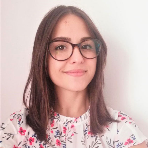
Luca Planat
CEO, Silent Waves
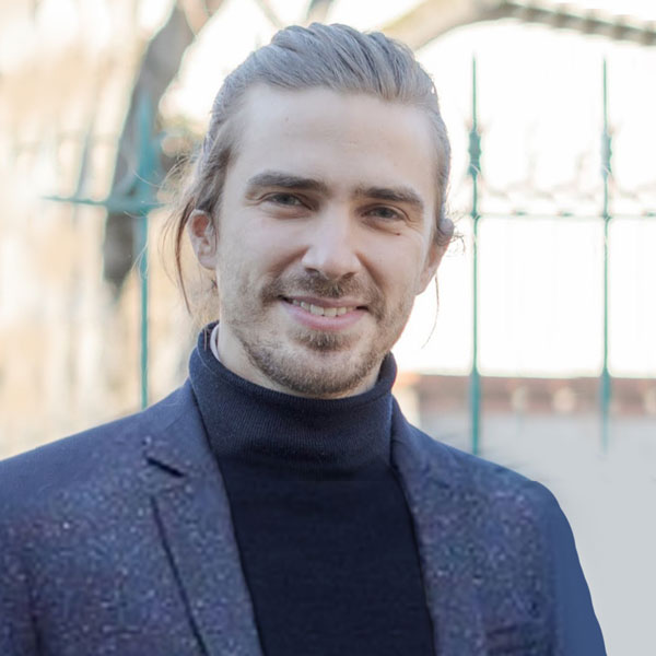
Luca Planat
CEO, Silent Waves
Bio:
Luca Planat is the CEO of Silent Waves, a startup company based in Grenoble developing, manufacturing and commercializing readout hardware for quantum computing.
Luca Planat owns an engineer degree (2016) from Grenoble INP Phelma and did a PhD in quantum physics between 2016 and 2020 at the Institut Néel, Grenoble, France. During his PhD, he focused on the development of wideband, near quantum limited, microwave amplifiers. These amplifiers are key pillars for large-scale quantum processor readout since they provide very high signal noise ratio over several gigahertz bandwidth. Early 2022, Luca Planat has co-founded Silent Waves, together with his former PhD supervisor, Nicolas Roch, and Baptiste Planat.
Abstract:
Superconducting parametric amplifiers have added noise about five times lower than current commercial microwave amplifiers based on high electron mobility transistors (HEMT). Used as pre-amplifiers with HEMT-based microwave amplifiers, superconducting parametric amplifiers allow to reach system noise substantially lower than with a HEMT amplifier alone. With this lower system noise, high-fidelity single shot qubit readout becomes possible, making superconducting parametric amplifiers crucial for qubit operations.
We will see that superconducting parametric amplifiers based on Josephson junctions are good candidates to work as pre-amplifiers in qubit readout lines. Their gain and added noise allow to reach high readout fidelities. However, as the number of qubit is expected to grow significantly, scalability becomes an important point to consider; other parameters than gain and added noise become critical, such as saturation and bandwidth, since the number of qubits per readout line becomes relevant. Also, parameters which are not directly related to the amplifier’s characteristics must be taken into consideration: scalability, reproducibility and robustness of the manufacture process become also highly relevant as the demand for these amplifiers is correlated with the growing number of qubits.
In this presentation, we will see how the traveling-wave architecture for parametric amplifiers can address these issues, and how Silent Waves traveling-wave parametric amplifiers are a solution for teams studying qubits working at cryogenic temperature. Finally, we will see what can be done to improve our current amplifiers, the solutions to be explored to improve the manufacture process, and what are the limitations in terms of performance and scalability of the current readout line architecture.
Fabrice Debbasch
In charge of Quantum France 2030 Action, ANR
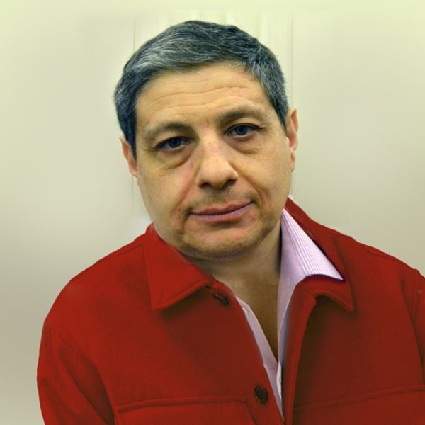
Fabrice Debbasch
In charge of Quantum France 2030 Action, ANR
Bio:
Fabrice is Responsable d’action quantique France 2023 at the ANR since March 2023. He began his carrer at the ENS Saint-Cloud and became Maitre de Conference at Sorbonne University in 1990. He has spent one year at CEA DAM, four years at DGA/DS/MRIS and is associate reearcher at the think tank IRIS. His scientific research, which was originally focused on stochastic processes, has shifted to quantum simulation in 2011. He is the author of some 80 scientific publications.
Abstract:
The quantum revolution is on our doorsteps and its impact on cybersecurity, and cryptography in particular, will be unprecedented. Quantum technologies represent an opportunity of having new secure cryptographic functions whether for random number generators (QRNG – Quantum Random Number Generators) or for cryptographic key distributions (QKD – Quantum Key Distribution). Quantum technologies also represent a threat to existing cryptographic algorithms, threat upon which anticipation work is being done through the study and deployment of quantum resistant cryptography (PQC – Post Quantum Cryptography). The quantum field has been labelled of strategic importance for France and thus, with its ‘Quantum strategy’, the French Government has been supporting the research and industrial communities in this field since 2
Pierre Desjardins
CEO, C12
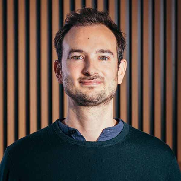
Pierre Desjardins
CEO, C12
Bio:
Pierre Desjardins holds a Master of Science degree from Columbia University (2013) and later worked for six years as a strategy consultant. He founded the startup C12 in 2020. C12 is leading the next materials leap in quantum computing.
Abstract:
Unlike other quantum computers, C12 uses carbon nanotubes as the fundamental building block of their processor. By combining the power of an ultra-pure material with an easy-to-manufacture semiconductor device, we are building the next-generation quantum computers.
Pierre Favier
System Engineer, Pasqal
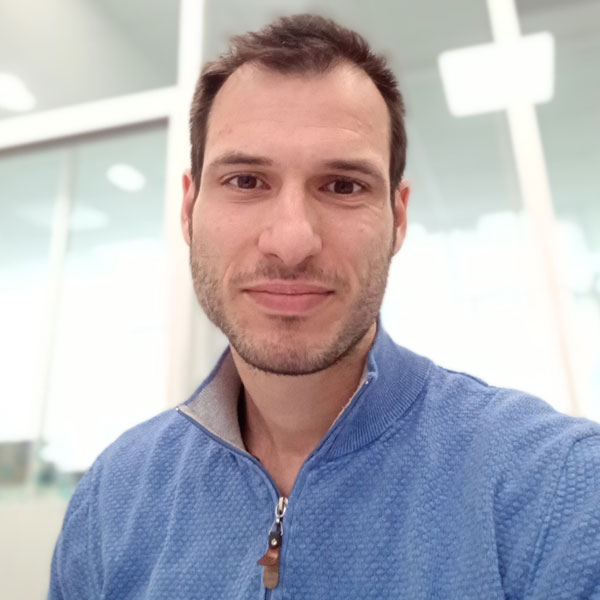
Pierre Favier
System Engineer, Pasqal
Bio:
After Physics studies in the Magistere of Fundamental Physics at Université Paris-Saclay, I made a PhD in laser-electron interactions in optical cavities at the IJCLab, in Orsay.
I then spent 5 years in the space industry as a technical leader and project manager for various laser systems and star trackers now installed on satellites.
Joining Pasqal in 2022 as a system engineer, I am involved in both the R&D and production teams to improve the performances of the current QPUs and lead the development of various sub-systems for the next generations of machines.
Abstract:
In recent decades, there has been remarkable progress in the control of isolated quantum systems. This mastery of quantum technology has led to its transition from purely fundamental research to potential industrial applications. The development of a functioning quantum computer is among the most ambitious technological goals of our time, with various platforms racing to achieve the best quantum processor. Among these platforms, arrays of neutral atoms held in optical tweezers are emerging as a promising quantum system, capable of both analogue and digital computation. This approach offers high spatial control of individual particles and holds the potential for large scalability. During this presentation, I will introduce the atom-based quantum processors that PASQAL, a spin-off company from the Institut d’Optique, is currently developing. The development of these processors builds upon experimental techniques pioneered by the Quantum Optics group at Laboratoire Charles Fabry. Their groundbreaking work resulted in the creation of a versatile quantum simulation platform capable of generating Hamiltonians using 2D and 3D arrays of single atoms trapped in optical tweezers. These atoms strongly interact with one another when excited to Rydberg levels, enabling the realization of a robust and powerful quantum simulator.
Sébastien Boissier
Head of R&D Semiconductor Quantum Devices, Quandela
Sébastien Boissier
Head of R&D Semiconductor Quantum Devices, Quandela
Bio:
Sebastien is an expert in the science and engineering of deterministic single-photon sources. He holds a PhD from Imperial College London on the coupling of single organic molecules to photonic micro-structures. Sebastien has a holistic experience in the development of quantum light sources, from the theoretical modelling and cleanroom fabrication to the optical characterisation and photonic packaging. Since joining Quandela in 2020, he has worked to industrialise the production cycle of quantum-dot based single-photon sources and optimise their performances. More recently, he has led the development of Quandela’s pilot-line for the fabrication of these sources and he is currently leading the R&D team conceiving next-generation devices.
Abstract:
Recent progress in the field of semiconductor quantum dots has recently enabled the fabrication of single-photon sources which are bright, pure and indistinguishable [1]. By placing dots in small optical cavities (in our case micropillar cavities), we both maximise the probability that photons are emitted into a single output mode as well as improving the quantum properties of the emission. Furthermore, with exquisite control over the charged-states of quantum dots (where a single electron or hole is trapped inside the dot), we can use the same technology to generate streams of photons which are sequentially entangled to one another [2]. This versatile platform is now reaching a level of maturity to enable many technologies of the 2nd quantum revolution, including photonic quantum computing. In this talk, I will present Quandela’s approach to emitter-based single-photon sources and describe how they are being put to use in the first European photonic quantum computer available on the cloud.
[1] Bright Polarized Single-Photon Source Based on a Linear Dipole. Phys. Rev. Lett. (2021). https://doi.org/10.1103/PhysRevLett.126.233601
[2] High-rate entanglement between a semiconductor spin and indistinguishable photons. Nat. Photon. (2023). https://doi.org/10.1038/s41566-023-01186-0
Ségolène Olivier
Quantum Photonics Program Manager, CEA-Leti
Ségolène Olivier
Quantum Photonics Program Manager, CEA-Leti
Bio:
Segolene Olivier is currently leading the quantum photonics program at CEA-Leti for applications in quantum communications and quantum computing.
She received her PhD in 2002 from the University of Paris in the field of optoelectronics and was hired at CEA-Leti in 2003 as a process and device R&D engineer. She developped her expertise in various fields such as III-V integrated photonics, microelectronic interconnects and optical data storage before she joined the silicon photonics lab in 2012. Since then, she has led several projects in collaboration with academic or industrial partners, dedicated to the development of active and passive silicon photonics components, hybrid III-V on Si lasers and integrated transmitters on silicon for WDM telecom and datacom applications. From 2016 to 2019, she was coordinating H2020 European project COSMICC on the development of Tb/s Silicon photonics transmitters for CWDM communications in datacenters. In 2018, she started exploring new emerging applications fields and launched a research activity in integrated quantum photonics.
Abstract Tomorrow’s Cybersecurity:
The future advent of quantum computers poses a serious threat on the security of current encryption algorithms used to transmit sensitive data in our communication networks. Building quantum-resistant security is therefore essential. Quantum cryptography offers absolute security, guaranteed by the laws of quantum physics. First implementations of quantum secure communication links are being demonstrated worldwide with bulky quantum key distribution systems. Miniaturization of those systems through the development of integrated components and circuits is key for the future large-scale deployment of a global quantum communication network, compatible with the existing fibre infrastructure. This talk will review the main challenges associated with the development of silicon photonics quantum integrated components meeting the requirements of advanced quantum key distribution protocols.
Abstract Quantum Computing:
Photonic qubits are a promising approach for quantum simulation and computing, providing a number of key advantages, such as insensitivity to their environment, hence no decoherence, and high connectivity. Remarkably, the use of photonic qubits has recently led to the demonstration of a quantum computing advantage. On the path towards the development of a practical large-scale quantum computing hardware, silicon photonics provides a low-cost, robust and scalable technology. This talk will review the main challenges associated with the development of silicon photonics quantum integrated components for generation, encoding, processing and detection of photonic qubits.
Frederic Barbaresco
Quantum Algorithms Segment Leader, THALES
Frederic Barbaresco
Quantum Algorithms Segment Leader, THALES
Bio:
F. Barbaresco is "Quantum Algorithms Segment Leader" in charge of coordination of THALES Quantum Algorithms R&T activity between Business Lines and TRTs (Thales Research & Technology), and of partnerships elaboration with deep-tech start-ups, academic labs and industries on quantum Algorithms & Computing.
F. Barbaresco coordinates BACQ project led by THALES from LNE MetriQs program on "Applications-oriented Benchmarkings of Quantum Computers". F. Barbaresco has organized in May 2023 a TERATEC TQCI (Teratec Quantum Computing Initiative) seminar with LNE on "Overview of upcoming application-oriented benchmarks for quantum computing in France and abroad" with more than 200 participants.
He has organized in 2023 the THALES International Quantum Hackathon jointly in FR, UK, GE, CAN & SG involving 58 participants in 10 teams working on 10 THALES use-cases with 9 QPU providers. He supervises THALES/EDF agreement on Quantum Algorithms for PDE solvers for Electromagnetic Simulation for THALES use-cases.
He has managed first benchmark of Quantum Algorithm for Radar Waveform Optimization QUBO problem on Quantum Annealer and its extension on NISQ with QAOA Algorithm. THALES representative at European QuIC (Quantum Industry Consortium) fon the state-of-the art. THALES representative at the AI Expert Group of ASD (AeroSpace and Defense Industries Association of Europe).
2014 Aymée Poirson Prize of the French Academy of Science for the application of science to industry. Ampère Medal, Emeritus Member of the SEE, and President of the SEE ISIC club "Information and Communication Systems Engineering". General Chair of the "Geometric Science of Information" international conference.
Graduated from CentraleSupelec French High-Engineering School in 1991.
Kenzo Bounegta
General Manager, Le Lab Quantique
Kenzo Bounegta
General Manager, Le Lab Quantique
Bio:
After studying at HEC Paris and École Polytechnique, Kenzo Bounegta worked at the Quantonation venture capital fund before becoming General Manager of Le Lab Quantique. Le Lab Quantique is a non-profit organization whose mission is to promote quantum technologies in France and internationally. It currently has over 50 member organizations. In order to create synergies between public and academic actors, large groups and startups, Le Lab Quantique organizes events (workshops, hackathons, scientific and artistic exhibitions) bringing together all the actors of the ecosystem. It produces content to promote quantum technologies and help identify use cases, coordinates regional and national funding initiatives, and supports workforce development by connecting innovation and talent.
Le Lab Quantique also works with its partners to create Les Maisons du Quantique, a physical space for the development and federation of French quantum players.
Christophe Vuillot
CR, INRIA
Christophe Vuillot
CR, INRIA
Bio:
Christophe Vuillot received the Ph.D. degree in computer science from TU Delft, Netherlands, in 2020. Since 2021 he is Chargé de Recherche (junior researcher) at Inria, in Nancy, France. His research focuses on fault-tolerant quantum computation.
Abstract:
Building a fully fault-tolerant and universal quantum computer is a tremendous challenge. The task is at heart interdisciplinary: involving research level physics, mathematics and computer science on top of a multitude of engineering challenges across the stack. Multiplying in this complexity is the fact that the task is far from monolithic. There are many different choices and approaches to take and many different blueprints of quantum computers have been and continue to be proposed.
To swiftly navigate this complex landscape strong and interdisciplinary collaborations are an asset, in particular at the research level. After presenting the french research landscape and the collaborations between research institute, I will illustrate how different quantum fault-tolerant scheme could impact the architecture of a quantum computer.
Anne-Lise Guilmin
ATOS/Eviden
Anne-Lise Guilmin
ATOS/Eviden
Bio:
Anne-Lise Guilmin graduated from CentraleSupelec French High-Engineering School in 2009 and received her PhD in modeling and simulation of geomaterials in 2012 at Université Paris-Est. She worked for Schlumberger (now SLB) mainly on Reservoir Engineering software, enhancing their physical simulation capacity and their performance. In 2022 she joined Eviden (an atos business) as Quantum Computing Consultant bringing her expertise to private customers and academic labs. Among her missions, she is accompanying companies in their adoption of quantum computing (use case assessment, trainings, proofs of concept,...) and she is involved in several initiatives and projects with Evidens’s partners in France and Europe.
Olivier Tonneau
Partner at Quantonation, investment fund dedicated to quantum technologies, Quantonation
Olivier Tonneau
Partner at Quantonation, investment fund dedicated to quantum technologies, Quantonation
Bio:
A graduate from ESSEC business school, Olivier is partner at Quantonation, VC fund dedicated to Quantum Technologies. Previous experiences include 10 years as management consultant at Kearney, before joining French entrepreneur Charles Beigbeder as deputy CEO at his holding company, Gravitation.
Olivier is a board member at Multiverse Computing, Qnami, KETS Quantum Security, EvolutionQ, QC Design, Kipu Quantum, Cryptonext Security and the Quantum Industry Consortium.
Thimothée Silvestre
Foresight Expert, CEA
Thimothée Silvestre
Foresight Expert, CEA
Bio:
After studying Biotechnology Engineering, Timothée SILVESTRE worked as a biologist at the Swiss Institute for Experimental Cancer Research (ISREC) in Lausanne, and then as a research engineer at the Lyon Bioinformatics Center (CNRS), after obtaining a degree in Computer Engineering. After working on genetic sequence alignment algorithms as part of the European DATAGRID computing grid project led by CERN, he earned an MBA at IAE Lyon3. After serving as an innovation expert in sustainable construction at ARIST (Burgundy Chamber of Commerce), he led the SPORALTEC cluster specializing in sports innovation. He joined CEA in 2015 as head of the Ideas Laboratory, which he directed for 4 years, and is currently focusing on technology monitoring and foresight missions within CEA Y spot.
Abstract:
At Y SPOT, the open innovation center of CEA Grenoble, we believe that true disruption occurs at the crossroads of sectors. By leveraging the collective intelligence of CEA’s experts in digital, energy, and health, we have developed a unique 'Wide-Angle' approach to identify the technologies that will redefine our society. This presentation invites you to broaden your peripheral vision and embrace serendipity by exploring a landscape where Physical AI and robotics, the evolution of Datacenters, the rise of OpenHardware, and the frontier of Bio-computing intersect. Whether these shifts are already impacting our industries or shaping a long-term future, our goal is to provoke a shift in perspective, allowing you to think differently and anticipate the next wave of transformation
Tomorrow’s Cybersecurity
Marion Andrillat
Cybersecurity Strategic Partnership Manager, CEA-Leti
Marion Andrillat
Cybersecurity Strategic Partnership Manager, CEA-Leti
After a Microelectronics Engineer degree at CPE Lyon, Marion Andrillat has started her career at STMicroelectronics as a digital designer of “System On Chip” for the payed TV setup boxes and consumer smartphones. In 2011, with a postgraduate Advanced Master in Marketing and Technological Innovation at Grenoble Ecole de Management, she joined the CEA as Strategic Marketing Manager. Then she moved as Strategic Partnership Manager for Systems Division at CEA Leti. Since 6 years, she is specialized in Cybersecurity Strategic Partnership Management for a wide range of industrial applications such as transports, smart grids, medical, industry 4.0, security & defense… and various devices such as integrated circuits, embedded systems or industrial equipment’s.
Marie-Sophie Masselot
Partnership & European Affairs Manager, CEA-Leti
Marie-Sophie Masselot
Partnership & European Affairs Manager, CEA-Leti
Marie-Sophie Masselot is now in charge of European Affairs for Hardware Cybersecurity. She has been a business developer at CEA Leti DSYS (Systems Department) since January 2020, in charge of cyber-security technologies at both the hardware and embedded software level.
She joined CEA Leti in 2016, as an expert in IoT technologies in areas such as interoperability for smart cities. She is a referent at CEA Leti on subjects relating to research technologies applied to the field of mobility.
Previously, she managed Marketing positions at HPE (Hewlett Packard Enterprise) for 15 years, notably for the IoT (Internet of Things) offer of the Telecom business unit.
She is an engineer in computer science from INSA Lyon.
Jacques Fournier
Director of Cybersecurity Program, CEA-Leti
Jacques Fournier
Director of Cybersecurity Program, CEA-Leti
Jacques Fournier is the director of CEA Leti’s cybersecurity program and deputy head of the embedded systems’ division that encompasses 4 research labs working on cybersecurity. He is also the deputy director of the Grenoble Alpes Cybersecurity Institute and he leads the national PEPR project ARSENE on hardware and embedded software security. Prior to joining the CEA Leti, he held several technical positions in the security labs of smart card manufacturer Gemalto between 2001 and 2009. Jacques Fournier holds a PhD from the University of Cambridge, an engineering degree from CentraleSupélec and is an auditor of the Institut des Hautes Etudes de Défense Nationale (IHEDN).
Bernard Barbier
CEO, BBCYBER SAS
Bernard Barbier
CEO, BBCYBER SAS
Bio:
Bernard began his research career at CEA (French Atomic Agency), in charge of the development of new nuclear weapons. He has become an expert in digital simulation and supercomputers. He created and became the first CEA CIO in 2000.
For 10 years, Bernard worked at LETI at CEA Grenoble, where he was named director in 2003. The LETI with MINATEC is considered as one of the world leading research laboratories in the field of nanotechnologies.
In 2006 Bernard was appointed, by the President of the French Republic, Technical Director of the DGSE, the equivalent of the USA NSA. Thanks to his experience and his technical knowledge, he completely transforms French technical intelligence and establishes close links with his counterparts in Europe and the USA.
In 2014 Bernard is recruited by the CAPGEMINI group (220,000 employees in 60 countries) to coordinate at the group level, internal cyber security to deploy a high level of security and protection against cyber-attacks.
Bernard's areas of expertise are very extensive, Plasma physics, Supercomputing and simulation, Nanotechnology and nanoelectronics, Cryptology and cryptanalysis, Electronic warfare and Sigint (signal intelligence), Cyber operation, Cyber security and cyber defense, Cyber crisis management.
Thanks to his 40 very diversified professional years, Bernard created a very important network of relations, in defense, and in large French companies and more particularly with the CISO’s and CIO’s.
Bernard is one of the French pioneers of cybersecurity and cyberdefense. He has more than 25 years of experience in offensive and defensive areas. In 2007 he was a founder of the computer network operation concept in France and its application in intelligence and information warfare. His technical expertise and his diverse professional experience have allowed Bernard to fully modernize French technical intelligence and to build the foundations of the French cyber army.
Abstract:
Geopolitics of Cyber Security: The Strategic Consequences for Cyber Defense of the Ukraine-Russia War
the risks of cyber attacks have never been greater: for states and companies. The Ukraine-Russia war is an accelerator of threats, but also the attack surface which increases exponentially with the Internet of Things and 5G-6G. Artificial intelligence provides very effective cyber defense solutions but it will also increase the potential of attackers.
Megan Samford
VP & Chief Product Security Officer, Schneider Electric

Megan Samford
VP & Chief Product Security Officer, Schneider Electric
Bio:
Presently the only female CPSO for a major industrial, Megan is a security executive with a focus on industrial control systems security, critical infrastructure protection, and risk analysis. Megan drives the product security strategy and program for Schneider Electric’s Energy Management business.
Prior to Schneider Electric, Megan was the Global Director of Product Safety and Security for Rockwell Automation, Product Security Leader for GE Global Research and lead for the GE Product Security Incident Response Team. While working in the public sector, she served as the Commonwealth of Virginia’s Critical Infrastructure Protection Coordinator and Special Assistant for Homeland Security Projects within the Governor’s Offices of Tim Kaine and Bob McDonnell.
Megan brings a unique perspective to the security community, based on her diverse security background, with an interest in utilizing proven concepts from traditional critical infrastructure protection and emergency management foundations, such as Incident Command System and preparedness, and applying those to cyber, in particular for industrial control systems incident response.
She is currently the Chairperson for the ISA Global Cybersecurity Alliance. She is also leading a community-driven effort known as Incident Command System for Industrial Control Systems (ICS4ICS), which seeks to establish a common language for responding to cyber incidents and provide avenues for mutual assistance between organizations. Lastly, she is the Co-Chairperson of the Department of Homeland Security’s Control Systems Working Group (CSWG).
Megan has served on numerous boards, including Virginia Commonwealth University’s School of Electrical and Computer Engineering (ECE), Security Analysis and Risk Management Association (SARMA), Department of Homeland Security’s Control Systems Security Working Group (CSWG), Trusted Computing Group (TCG), and Virginia Aviation Security Advisory Council (VASAC). She is also a returning 2022 Program Chair for the RSA Conference, “Secure All The Things” track.
Megan holds a bachelor’s degree in homeland security and emergency preparedness as well as a master’s in public administration, both from Virginia Commonwealth University.
Abstract:
While work on machine learning and AI has been going on for some time now, AI has been propelled center stage with popular AI tools such as ChatGPT. Suddenly the possibilities for AI seem to be forefront in everyone’s mind. The trends and implications of AI will be discussed regarding what AI may represent in the way of new threats as well as how it could be used to augment security in industrial control system environments, including a short summary of Schneider Electric’s AI collaboration with CEA to create focused attention on cyber-attacks on OT systems.
Pierre-Alain Moellic
Research Engineer, CEA-Leti
Pierre-Alain Moellic
Research Engineer, CEA-Leti
Bio:
Pierre-Alain Moellic is a research engineer at CEA-LETI in the Security of Embedded Systems laboratory. He is member of a joint research team between CEA-LETI and Mines Saint-Etienne (IMT) at the Center of Microelectronic of Provence Georges Charpak (Gardanne) that gathers cutting-edge equipment for hardware security characterization and testing. His works essentially focus on the interaction between physical attacks and security of machine learning. He is the coordinator of PICTURE (ANR) dedicated to the security of embedded neural network models, the national coordinator for the European program InSecTT on "AIoT" and leads the "Security of AI" topic in the PULSE program (IRT Nanoelec).
Abstract:
The large-scale deployment of machine learning (ML) models in a large variety of hardware platforms raises many security issues methodically studied and demonstrated by both the adversarial and privacy-preserving ML communities. Nowadays, some worrying attacks are popular such as the adversarial examples that aim at optimally altering the inference inputs to fool the prediction of a state-of-the-art model, especially deep neural networks. Another important threat – known as model extraction - concerns the confidentiality of a protected black-box model that an adversary want to clone or steal its performance. Until recently, most of the attacks were considering a target model as a pure abstraction, relying essentially on API-based strategies, i.e. exploiting a set of inputs/outputs and some knowledge about the model and the data. In this talk, we highlight recent threats on implementation-based attacks that leverage software or hardware features of the a deployed model. More particularly, we describe adversarial attacks that directly alter the internal parameters stored in memory (e.g., DRAM or Flash) and physical attacks (side-channel and fault injection analysis) for model extraction. With such an attack surface, the development of defenses is as challenging as urgent and must be guided by sound and robust evaluation protocols.
Fabien Clermidy
Head of Systems Division, CEA-Leti
Fabien Clermidy
Head of Systems Division, CEA-Leti
Bio:
Fabien Clermidy is currently heading the system Division of CEA-LETI. He was previously leading the digital architecture and IC design division.
The main activities of his division spread from power modules development to hardware cybersecurity, including sensors system design and new telecommunication scheme. The main applicative domains are automotive, factory of future, energy, telecommunications, security and defense.
Fabien holds a PhD, a thesis supervisor degree and is a CEA research director. He has published more than 100 papers including in the greatest conferences such as ISSCC, VLSI, DAC, DATE or IEDM. He is also author or co-author of 15 patents. Fabien is in the board of directors of the open Hardware Group leveraging on RISC-V open-source initiative.
Eric Saliba
Head of the Scientific and Technical Division, ANSSI
Eric Saliba
Head of the Scientific and Technical Division, ANSSI
Bio:
Eric Saliba is Head of the Scientific and Technical Division of the National Agency for Information Systems Security (ANSSI). ANSSI's scientific and technical division brings together the laboratories in which the experts ensure the definition and maintenance of the agency's technical standards, and provide their expertise to the various ANSSI structures as well as to their beneficiaries. Eric has worked for more than twenty years on upstream studies and major research and development or production projects, as an expert and technical manager within large companies in the defence and cybersecurity industrial sectors. Engineer in microelectronics and telecommunications, he participated in the design and the development of several secure components and embedded products or systems for civil and government use.
Simon Moore
Professor of Computer Engineering, University Cambridge
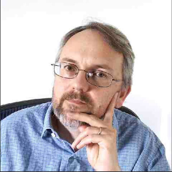
Simon Moore
Professor of Computer Engineering, University Cambridge
Bio:
Simon Moore is a Professor of Computer Engineering at University of Cambridge, Department of Computer Science and Technology (previously The Computer Laboratory) where he conducts research and teaching in the general area of computer architecture with particular interests in secure and rigorously-engineered processors and subsystems. Since 2010, he has led the microarchitecture work on CHERI for a number of ISAs including RISC-V. He is vice-chair of the CHERI special interest group at RISC-V International.
Ségolène Olivier
Quantum Photonics Program Manager, CEA-Leti

Ségolène Olivier
Quantum Photonics Program Manager, CEA-Leti
Bio:
Segolene Olivier is currently leading the quantum photonics program at CEA-Leti for applications in quantum communications and quantum computing.
She received her PhD in 2002 from the University of Paris in the field of optoelectronics and was hired at CEA-Leti in 2003 as a process and device R&D engineer. She developped her expertise in various fields such as III-V integrated photonics, microelectronic interconnects and optical data storage before she joined the silicon photonics lab in 2012. Since then, she has led several projects in collaboration with academic or industrial partners, dedicated to the development of active and passive silicon photonics components, hybrid III-V on Si lasers and integrated transmitters on silicon for WDM telecom and datacom applications. From 2016 to 2019, she was coordinating H2020 European project COSMICC on the development of Tb/s Silicon photonics transmitters for CWDM communications in datacenters. In 2018, she started exploring new emerging applications fields and launched a research activity in integrated quantum photonics.
Abstract Tomorrow’s Cybersecurity:
The future advent of quantum computers poses a serious threat on the security of current encryption algorithms used to transmit sensitive data in our communication networks. Building quantum-resistant security is therefore essential. Quantum cryptography offers absolute security, guaranteed by the laws of quantum physics. First implementations of quantum secure communication links are being demonstrated worldwide with bulky quantum key distribution systems. Miniaturization of those systems through the development of integrated components and circuits is key for the future large-scale deployment of a global quantum communication network, compatible with the existing fibre infrastructure. This talk will review the main challenges associated with the development of silicon photonics quantum integrated components meeting the requirements of advanced quantum key distribution protocols.
Abstract Quantum Computing:
Photonic qubits are a promising approach for quantum simulation and computing, providing a number of key advantages, such as insensitivity to their environment, hence no decoherence, and high connectivity. Remarkably, the use of photonic qubits has recently led to the demonstration of a quantum computing advantage. On the path towards the development of a practical large-scale quantum computing hardware, silicon photonics provides a low-cost, robust and scalable technology. This talk will review the main challenges associated with the development of silicon photonics quantum integrated components for generation, encoding, processing and detection of photonic qubits.
Vincent Cachard
Hardware Security Group Manager, CEA-Leti & Director, CEA-Leti ITSEF
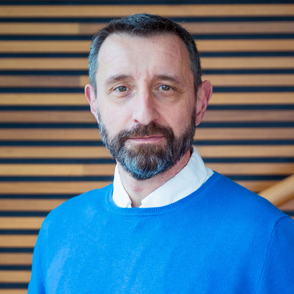
Vincent Cachard
Hardware Security Group Manager, CEA-Leti & Director, CEA-Leti ITSEF
Abstract:
In a swift evolving digital world, cybersecurity threat is becoming a major concern for product and services providers and users.
In such respect, when it comes to hardware cybersecurity challenges, one of the most important seems to remain the capability to reliably identify and quantify products and services weaknesses along with threats evolution.
This crucial step needs then to be put in regard to the product environment, product design, and product and data sensitivity in order to be able to set up the appropriate protection techniques guaranteeing optimized Confidentiality, Authenticity, Integrity and Availability.
In this talk, we will review the main hardware security assessment techniques and their characteristics and how CEA LETI handles the electronic security testing challenge for hardware components and systems.
Fabrice Isnard
Chief Operating Officier, FARE—RESEAU DEF
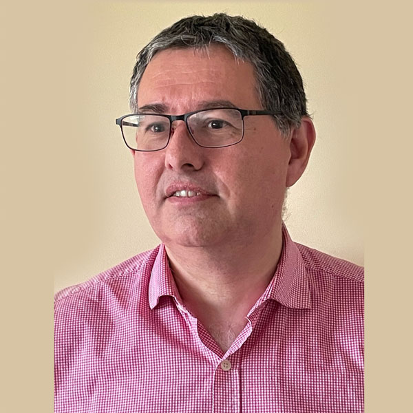
Fabrice Isnard
Chief Operating Officier, FARE—RESEAU DEF
Bio:
Fabrice ISNARD joined Reseau DEF in 2009 as a R&D coordinator, to define and develop a new generation of fire security systems, in line with the new challenges of safety, connectivity and maintenance which have been raised for these systems. Since 2021, he has been appointed COO of FARE, the company in Reseau DEF in charge of development and production of smoke detectors.
After an engineering degree in 1993 in Ecole Centrale Paris, he has been always in charge of development of products with security requirements to protect people and goods. he has started in Groupe FAYAT in the world of traffic light controllers. After he works in the automative industry and develop in Valeo acces controls and immobilizer systems. Then he reached the reseau DEF in the domain of fire security systems to launch new solutions always with the same requirement of security and safety for people, even with connected solutions.
David Richetto
Executive Director, STMicroelectronics
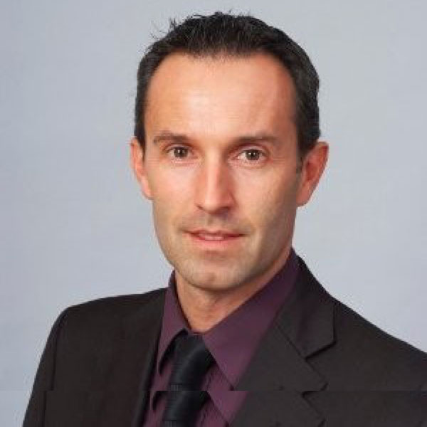
Eric Mercier
Telecom Line Director, CEA-Leti
Eric Mercier
Telecom Line Director, CEA-Leti
Eric Mercier is Telecom Line Director at CEA-Leti as well as Deputy Head of the Wireless Unit. He is active in industrial partnership developments towards technology transfer and also in managing internal CEA-Leti program, amongst which the FAMES WP10 dedicated to demonstrators. Graduated from ENSEEIHToulouse, France, in 1991, and with a 1st experience in the Optical Test Equipment at Wavetek (1992 – 1998, now VIAVI), his main focuses of interest have covered activities from Low-Power IoT transceiver solutions as Marketing & Application Manager for Atmel (1999 – 2006, now Microchip), and later as Project Manager & Laboratory Head Manager at CEA-Leti from 2006. As a promoter of CEA-Leti RF/mmW research activities, he is committed to market & societal needs for next Telecom generation towards new technologies development, understanding how forthcoming scientific developments can be valued to that end.
Thierry Collette
Director, Information Science and Technology Group, Thales
Thierry Collette
Director, Information Science and Technology Group, Thales
Bio:
Thierry Collette is director of the Information Sciences and Techniques research group at Thales Research and Technology. The group focuses on disruptive technologies such as embedded and trusted AI, open hardware, continuum computing, quantum computing, etc, in order to facilitate their adoption and integration into future Thales products. Before, Thierry Collette led the technology development division for embedded computing and components at CEA Leti & List for eight years. He contributed to set up the European Processor Initiative (EPI) in cooperation with industrial and academic partners. Previously, he was deputy director in charge of programs and strategy at CEA List. He holds several patents on multi-core architectures and has contributed to the creation of more than 10 startups, including Kalray and SiPearl. He holds an engineering degree in computer science and electrical engineering and a PhD in microelectronics.
Andreas Mitrakas
Head of Unit – Market, Certification & Standardisation, European Union Agency for Cybersecurity (ENISA)
Andreas Mitrakas
Head of Unit – Market, Certification & Standardisation, European Union Agency for Cybersecurity (ENISA)
Bio:
Dr. Andreas Mitrakas is Head of Unit “Market, Certification & Standardisation” in the European Union Agency for Cybersecurity (ENISA). He co-chairs the Stakeholders Cybersecurity Certification Group (SCCG). At ENISA he has previously held various posts in operational management and general management.
Prior to joining ENISA, Andreas served as General/Senior Counsel in Globalsign, Verizon/Ubizen.
Andreas is a qualified lawyer and holds a doctorate in business procedures, information technology and Law (Erasmus University of Rotterdam), a M.Sc. in Strategic Quality Management (University of Portsmouth) a LL.M. in Computer science and Law (Queen’s University of Belfast) and a first degree in Law (University of Athens).
Abstract:
This presentation provides a policy overview of the cybersecurity certification framework and the accomplishments of the preparation of drfat candidate cybersecurity certification schemes. It also presents complementary and support actions concerning standardization and the provisions of the proposed amendments to the Cybsersecurity Act.
Christophe Laurencin
Architecture, Security & Labs Director, STMicroelectronics
Christophe Laurencin
Architecture, Security & Labs Director, STMicroelectronics
Bio:
I started as digital designer on MPEG decoder, 8-bit and 32-bit secure microcontrollers.
After 8 years of digital design I moved to the customer support for secure microcontrollers, in this context I learnt a lot on security, chip hacking and cryptography.
I supported ST's customers in a context of hacking, this helps a lot to understand how hackers can be very efficient.
We always succeeded in strengthening our products and satisfying the customer in such exposed markets.
This was also an good opportunity to learn how to define product by understanding customer needs.
Following this experience I same back to a development job by leading a Security architecture team.
I'm now in charge of architecture teams for Secure Microcontrollers circuit and I also have the responsibility of Security lab being in charge to apply physical attack on product before launching the security certification phase.
Fabrice Debbasch
In charge of Quantum France 2030 Action, ANR

Fabrice Debbasch
In charge of Quantum France 2030 Action, ANR
Bio:
Fabrice is Responsable d’action quantique France 2023 at the ANR since March 2023. He began his carrer at the ENS Saint-Cloud and became Maitre de Conference at Sorbonne University in 1990. He has spent one year at CEA DAM, four years at DGA/DS/MRIS and is associate reearcher at the think tank IRIS. His scientific research, which was originally focused on stochastic processes, has shifted to quantum simulation in 2011. He is the author of some 80 scientific publications.
Abstract:
The quantum revolution is on our doorsteps and its impact on cybersecurity, and cryptography in particular, will be unprecedented. Quantum technologies represent an opportunity of having new secure cryptographic functions whether for random number generators (QRNG – Quantum Random Number Generators) or for cryptographic key distributions (QKD – Quantum Key Distribution). Quantum technologies also represent a threat to existing cryptographic algorithms, threat upon which anticipation work is being done through the study and deployment of quantum resistant cryptography (PQC – Post Quantum Cryptography). The quantum field has been labelled of strategic importance for France and thus, with its ‘Quantum strategy’, the French Government has been supporting the research and industrial communities in this field since 2
Alexandre Aubry
Cybersecurity Innovation Pilot, Stellantis
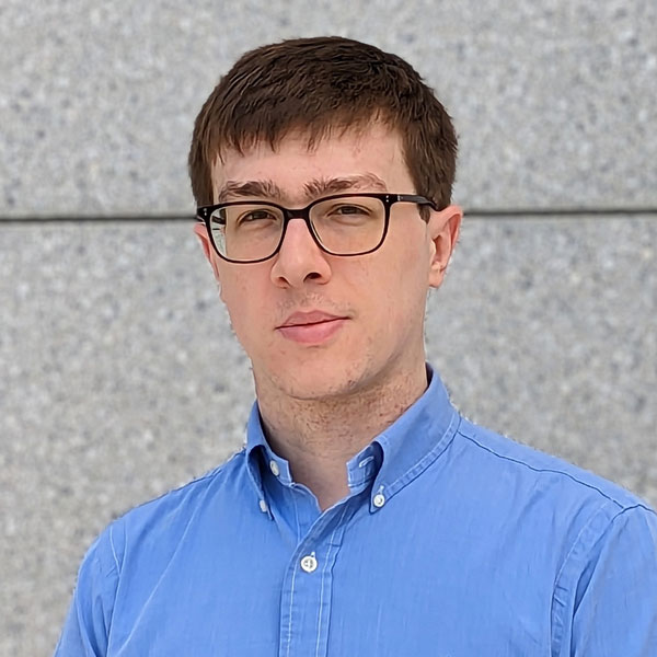
Alexandre Aubry
Cybersecurity Innovation Pilot, Stellantis
Bio:
Alexandre Aubry is an Innovation Pilot dedicated to Cybersecurity at Stellantis. He graduated in 2018 in Computer Science and Microelectronics from Mines Saint-Etienne. He started his career in Germany as a consultant working on a fusion-based automated parking system for high-end cars. Since 2020, he joined PSA Automobiles and was in charge of cybersecurity studies for the medium to long term vehicles and products. Now part of Stellantis Technology organization, his cybersecurity activities cover the connected, electric and autonomous vehicle as well as next generation electronics and services. He is passionate about both Cybersecurity and Automotive.
Sébastien Dauvé
Chief Executive Officer, CEA-Leti

Sébastien Dauvé
Chief Executive Officer, CEA-Leti
Bio:
Sébastien Dauvé was named CEO of CEA-Leti effective on July 1, 2021, after more than twenty years of experience in microelectronics technologies and their applications, including clean mobility, medicine of the future, cybersecurity, and power electronics.
Sébastien Dauvé started his career at the French Armament Electronics Center, where he worked on developing synthetic-aperture radar. In 2003, he joined CEA-Leti as an industrial transfer manager and supervised several joint research laboratories, in particular with the multinational Michelin.
In 2007, Sébastien Dauvé became a laboratory manager, then head of an R&D department in the area of sensors applied to the Internet of things and electric mobility. During this time, he supported the dissemination of new technologies in industry, including the automotive industry (Renault), aeronautics, national defense (SAFRAN), and microchips with the industry leader Intel. He played an active role in the creation of start-ups in application fields ranging from health to infrastructure security, leading to dozens of new jobs. In 2016, he became Director of the CEA-Leti Systems Division.
From sensors to wireless communication, Sébastien Dauvé has played an active role in the digital transformation, focused on coupling energy frugality and performance. He has made cross-disciplinary approaches central to innovation by harnessing the expertise of talented teams with diverse backgrounds. Their goal is to provide technological tools for meeting the major societal challenges of the future.
Sébastien Dauvé is a graduate of the French Ecole Polytechnique and the National Higher French Institute of Aeronautics and Space (ISAE-SUPAERO).
Memory for Edge Computing
Elisa Vianello
Edge IA Program Manager, CEA-Leti
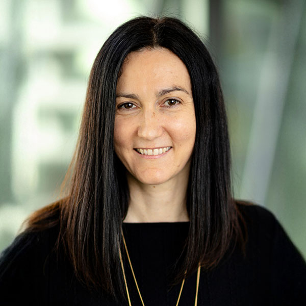
Elisa Vianello
Edge IA Program Manager, CEA-Leti
Bio:
Elisa is a senior scientist at CEA-Leti. She joined the institute in 2011 after spending one year on the research staff at Fondazione Bruno Kessler, Trento. Her current research interests concern the development of new technologies for bio-inspired neuromorphic computing, with special focus on resistive switching memory devices. She has authored or co-authored 4 book chapters and more than 100 technical papers.
She is coordinator of the "MeM-Scales" (2020-2022) European project (H2020) focused on the codevelopment of a novel class of algorithms, devices and circuits that reproduce multi-timescale processing of biological neural systems. In 2022 she won an ERC Consolidator Grant on "Heterogeneous integration of imprecise memory devices to enable learning from a very small volume of noisy data".
She is member of the editorial board of the Neuromorphic Computing and Engineering IOP Science journal (2019-now); associate editor of the Special issue on Emerging Materials in Neuromorphic Computing, AIP APL Material (2020); associate editor of the IEEE Trans. on Circuits and Systems –II (2020-2021).
She received the PhD in Electrical Engineering from the Università degli Studi di Udine (Italy) and the Grenoble Institute of Technology (INPG, France) in 2010.
François Andrieu
Head of Memory & Computing Laboratory, CEA-Leti
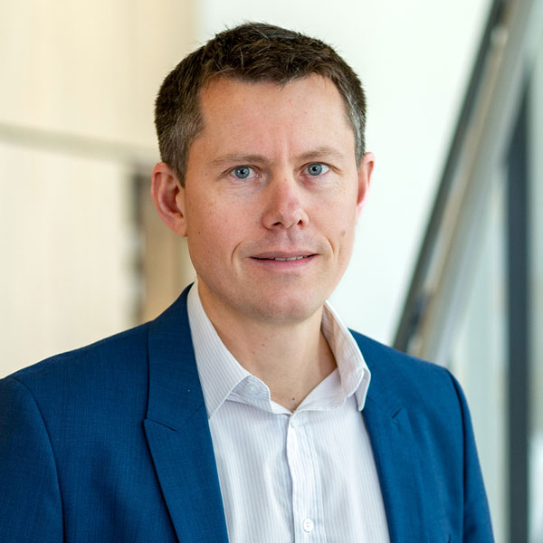
François Andrieu
Head of Memory & Computing Laboratory, CEA-Leti
Dr. François Andrieu is CEA fellow and the head of Laboratory “Nano-devices for Memory and Computing” at CEA-Leti, Grenoble, France.
He has been strongly involved in the development of the Fully-Depleted-Silicon-On-Insulator (FD-SOI) CMOS technology at Leti and with STMicroelectronics, where he was assigned between 2012-2015 in the process-integration and technology-to-design groups. His fields of interest are: NVM Resistive-RAM, In-Memory-Computing, advanced CMOS transistors, 3D-sequential integration.
He is the author or co-author of more than 34 patents, 240 conference abstracts or refereed journal articles, 11 invited papers and 3 book chapters. He received the IEEE senior grade in 2018, the European ERC consolidator grant in 2019 and the IEEE/SEE Brillouin award in 2018.
Johannes Müller
SMTS Global Technology & Development, GlobalFoundries
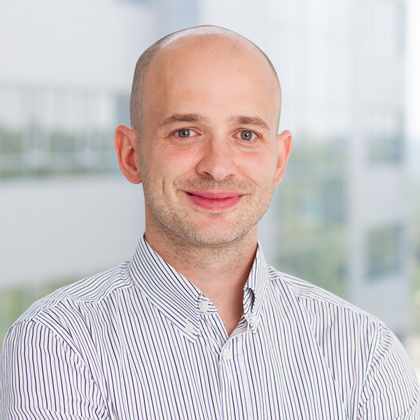
Johannes Müller
SMTS Global Technology & Development, GlobalFoundries
Bio:
Dr. Müller is a Senior Member of Technical Staff in the TD Organization of GlobalFoundries and is currently driving next-generation MRAM stack development activities. Previously he was acting as the overall-integrator for the now qualified and ramped embedded 22FDX® STT-MRAM technology. Prior to joining GlobalFoundries Dr. Müller was heading the group for Non-Volatile Memories at Fraunhofer IPMS (formerly known as CNT) overseeing direct industry collaborations and European projects focused on FRAM, FeFET, STT-MRAM, RRAM, and FLASH.
Dr. Müller holds a diploma degree in Applied Natural Science from the Technical University Freiberg and a Ph.D. degree in Electrical Engineering from the Technical University of Dresden. To date Dr. Müller has authored/co-authored >130 peer-reviewed journal papers, contributions to international conferences and patents (h-index: 49). As panelist, invited speaker or short course tutor Dr. Müller has served the scientific community at e.g. IEDM, IMW, ECS, NVMTS, SSDM, SISC, INTERMAG, etc., and as an expert in his field contributed to the ERD Working Group of the former ITRS.
Abstract:
STT-MRAM has successfully entered the embedded NVM market as an eFLASH replacement at the 2X nm node. This first entry point is mainly focused on MCUs targeted for low-power consumer/industrial IoT applications. However, with the now rapid acceleration of fully electrified mobility and autonomous driving on the horizon the automotive sector as well has a growing need for more performant and cost-effective chip technologies. Due to the fading scalability roadmap of the highly trusted eFLASH a new automotive capable NVM solution must be established to serve the needs of future technology nodes. Through its qualification and volume ramp STT-MRAM has proven to be the most reliable amongst the former emerging memories and can be viewed as the predestined successor of eFLASH in this demanding application space.
In this talk we will review the challenges and required innovations on the road towards an automotive capable embedded STT-MRAM solution. Especially the readability across temperature as well as the more stringent requirements in terms of chip failure rate require significant advancements from the first generation of eMRAM. Component failure in the field is not an option, so starting already inline, a solid line of defense needs to be established.
This work was funded in the framework of IPCEI-EUROFOUNDRY by the Federal Ministry for Economics and Energy and by the State of Saxony.
Sébastien Ricavy
Memory Architect, CEA-Leti
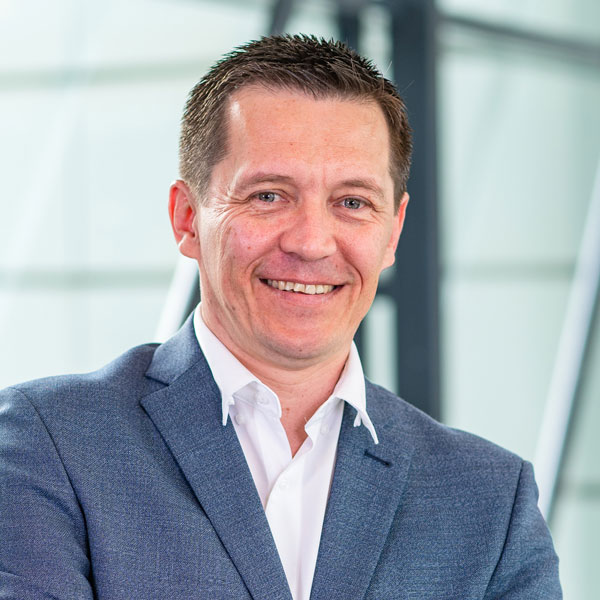
Sébastien Ricavy
Memory Architect, CEA-Leti
Bio:
Sebastien Ricavy (1977, Aug. 13) received the M.Sc. degree in electrical engineering and computer sciences fields in 2001 from Grenoble Alpes University, Grenoble, France.
He started his career focusing on design of standard cells and memories on SOI technologies (PD/FDSOI technologies) at SOISIC SA. From 2006 to 2018, he worked at ARM LTD where he was involved in SRAM, register files or VROM design activities as Senior Memory Technical Lead role or Memory Team Manager. Since 2019, he has been working as Memory Research Engineer at CEA, Grenoble, France. His research activities include various type of non-volatile technologies such as OxRAM, FeRAM or PCM designs.
Abstract:
Resistive RAM (RRAM) is a promising candidate to replace NOR eFlash in sub-40nm CMOS technologies. It offers low cost, high-speed and low-voltage embedded non-volatile memories compatible with CMOS back-end process. However, the stochasticity of RRAM programming limits the intrinsic performance of memory arrays without the use of advanced design assist techniques. The recent industrial adoption of RRAM in some major foundries has been done through a significant involvement of circuit design community to boost both the read-margin (RM) and endurance, while reducing the energy consumption.
In this talk, we will review different RRAM design assist techniques and we will demonstrate their impact on enhancing the intrinsic RRAM performance. Based on representative RRAM macro (130nm CMOS), statistic (176kb) and endurance (1M cycles) characterizations, we will show how pairing both process development and design solutions can push the intrinsic RRAM performance to the next level.
Stefan Müller
CTO, Ferroelectric Memory Corp. (FMC)
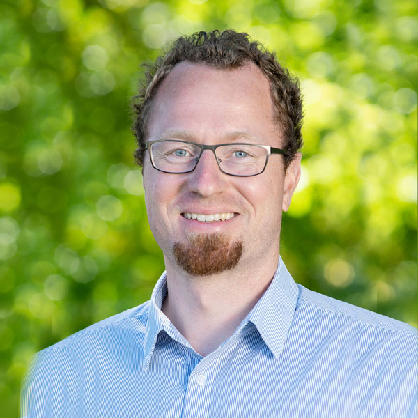
Stefan Müller
CTO, Ferroelectric Memory Corp. (FMC)
Bio:
Dr. Stefan Müller received the joint master's degree in Microelectronics from Technical University Munich, Germany, and Nanyang Technological University Singapore in 2011. He also holds a German diploma degree in Mechatronics and Information Technology as well as a bachelor's degree in Mechanical Engineering both from Technical University Munich, Germany (2011/2008). In 2011, he joined NaMLab gGmbH, a research institute of University of Technology Dresden. In 2015, he received his PhD degree for his work on HfO2-based ferroelectric devices. In 2016, he co-founded FMC-The Ferroelectric Memory Company where he currently holds the position of CTO.
Abstract:
Over the last decade, more and more research and development effort has been assigned to memory devices based on ferroelectric hafnium oxide (FE-HfO2). This was caused by the fact that FE-HfO2 itself was the first ferroelectric material that is 100% compatible to today's state-of-the-art semiconductor manufacturing environments and it is scalable down to 5 nm film thickness.
In this talk, we will review the different memory cell development directions that FE-HfO2 has opened up and for which first demonstrations exist. Memory cells will be benchmarked against each other, and their suitability for different application spaces will be discussed. Moreover, the suitability of different ferroelectric memory cells for analog or digital computing will be presented.
Hitoshi Saito
Sr. Dir. of Sales & Marketing Div. / Dir. of Energing Memory Dept., Fujitsu Semiconductor Memory Solution Limited
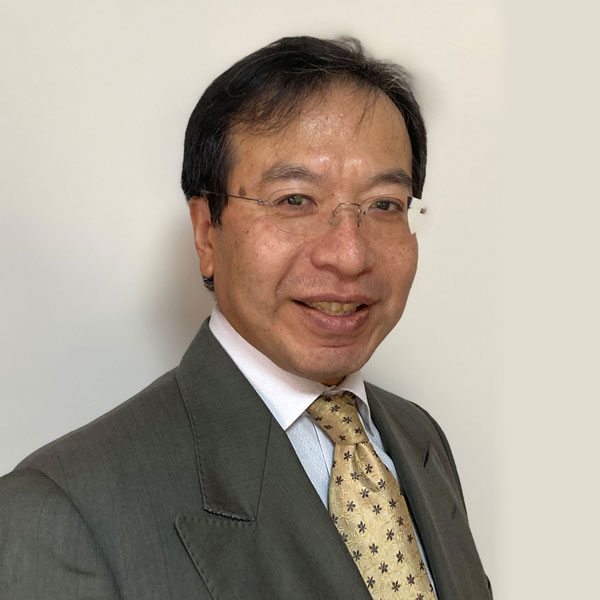
Hitoshi Saito
Sr. Dir. of Sales & Marketing Div. / Dir. of Energing Memory Dept., Fujitsu Semiconductor Memory Solution Limited
Bio:
Hitoshi Saito joined Fujitsu Limited in 1990 after earning a bachelor's degree in electrical engineering from Tokyo University of Agriculture and Technology. He has been contributed in the development of DRAM, LOGIC, NAND, FeRAM, and NRAM. Since 2023 he has been Sr. Dir. of Sales & Marketing Div. / Dir. of Energing Memory Dept. at FUJITSU SEMICONDUCTOR MEMORY SOLUTION LIMITED. His recent interest is processes, devices and marketing in emerging memory. He has or had 23 patents on semiconductors. He is the author or co-author of 11 articles on FeRAM or NRAM.
Abstract:
FeRAM is a nonvolatile memory which holds data by a ferroelectric capacitor with remanent polarization. FeRAM has five main advantages: low write power consumption, high write endurance, high write speed, long data retention and low temperature operation. Current FeRAM applications are automotive, wearables, meters, FAs, and counters. We are developing HZO FeRAM with low voltage writing and high writing endurance. I will describe the application of FeRAM in the near future.
Ilan Sever
VP R&D, Weebit Nano
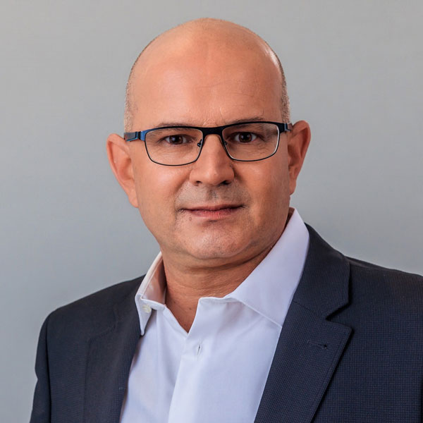
Ilan Sever
VP R&D, Weebit Nano
Bio:
Mr. Sever has over 25 years of design & project-management expertise in the field of Non-Volatile-Memory, Semiconductor IP, and SOC design. Prior to joining Weebit-Nano, Mr. Sever served as the Memory-Group CTO and Subsidiary GM at Dolphin-Design, leading the development of numerous memory architectures, as well as innovation projects in the fields of security, rad-hard memories, and RISC-V memory subsystems.
He previously managed the VLSI activities of Sandlinks Systems - a company in the field of IoT, developing a breakthrough Low-Power, Mixed-Signal/RF SOC. In his previous roles, Mr. Sever was Director of IP & Libraries at Tower Semiconductors and Design Manager of Flash-Memory at ST Microelectronics. Mr. Sever holds a BSCEE from the Technion - Israeli Institute for Technology and has several granted patents and awards.
Andrea Redaelli
PCM Process Architecture Technical Director - Fellow at STMicroelectronics
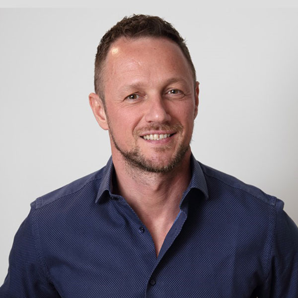
Andrea Redaelli
PCM Process Architecture Technical Director - Fellow at STMicroelectronics
Bio:
Andrea received the Laurea and Ph.D. degrees in electronic engineering from the Politecnico di Milano, Italy. During the Ph.D., he worked on Phase Change Memories in the Department of Electrical and Electronic Engineering (Politecnico di Milano), collaborating with the Non-Volatile Memory Technology Development Group of STMicroelectronics, Agrate Brianza. In 2007 he joined STMicroelectronics working on advanced technologies for Non-Volatile Memories. From 2008 to 2013 he worked as cell lead engineer on 45 and 28 nm PCM technology developments, firstly as a Numonyx employee and then joining Micron Technology. In the same years, Andrea cooperated with the Department of Electrical Engineering, Politecnico di Milano, in holding master classes on electronics and signal conditioning. From 2014 to March 2020, he worked on 3DXpoint technologies, in charge of the cell development at the most advanced scaled nodes. Since April 2020, Andrea is a fellow in STMicroelectronics, leading the cell development of embedded PCM technologies. Andrea is author and co-author of more than 60 papers and more than 130 granted US patents, resulting in a h-index of 29 according to google scholar.
Giuseppe Desoli
Company Fellow, Senior Director of Artificial Intelligence & Embedded Architectures, STMicroelectronics
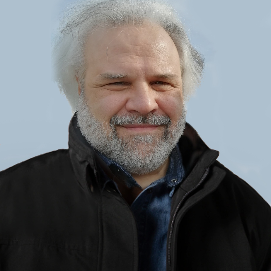
Giuseppe Desoli
Company Fellow, Senior Director of Artificial Intelligence & Embedded Architectures, STMicroelectronics
Bio:
Giuseppe Desoli holds a Master and PhD in Electrical Engineering from the University of Genoa. From 1995 to 2002, he worked at Hewlett-Packard Laboratories, developing VLIW microprocessor architectures, compilers, and tools. In 2002 joined STMicroelectronics as an R&D Director and lead microprocessor architect, pioneering multiprocessor systems for embedded SoCs. Since 2012, he is serving as Company Fellow and Chief Architect for the System Research & Application central R&D group, he is the chairman of the ST scientific committee and coordinator for the ST’s Artificial Intelligence Affinity Team, leading the development of different technologies in the field of HW accelerated AI and In-Memory-computing for advanced deep learning applications. He has co-authored over 70 scientific publications and holds more than 60 patents.
Masanori Tsukamoto
Senior Manager, Sony Semiconductor Solutions
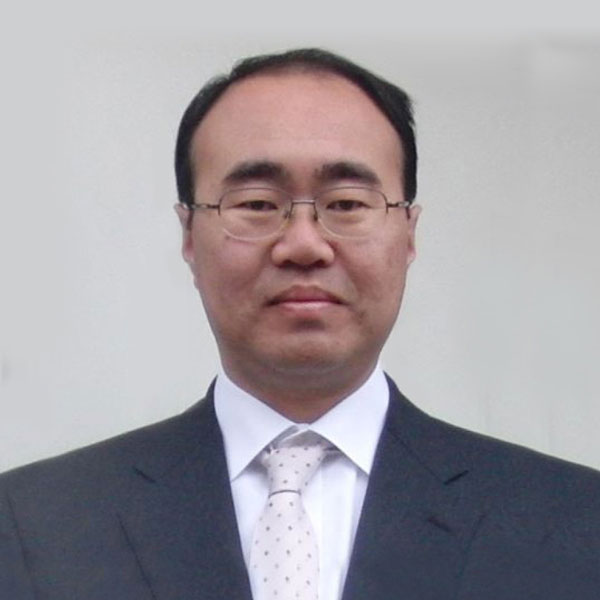
Masanori Tsukamoto
Senior Manager, Sony Semiconductor Solutions
Bio:
Masanori Tsukamoto received the B.S. and M.S. degrees in electric engineering from Chiba University, Chiba, Japan, in 1988 and 1990, respectively. Since 1990, he has been with the semiconductor business group, Sony Corporation, Atsugi, Japan, where he has been working on the technology development and manufacturing operation of 250-, 180-, 90-, 45- and 22nm-node SRAMs and CMOS LSIs. He is currently a Senior Manager in the memory technology department, Sony Semiconductor Solutions Corp. and engaged in the development of the emerging memory device.
Abstract :
For the edge AI applications, emerging memories such as RRAM, MRAM are potential candidates to address these concerns. However, these memories require high write energy consumption due to a current driven switching. Recently, a hafnium oxide based ferroelectric technologies have been strongly focused. We experimentally demonstrate 1T1C FeRAM memory array for the first time.
Deep neural network (DNN) inference for edge AI requires low power operation. We demonstrated it by implementing massively parallel matrix-vector multiplications (MVM) in the analog domain on highly resistive memory array. We propose a 1T1R compute cell (1T1R-cell) using FeFET and tunneling junction of MΩ resistor (MOR) for analog in-memory computing (AiMC).
Manuel Le Gallo
Staff Research Scientist, IBM
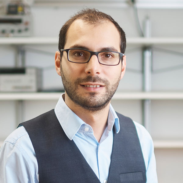
Manuel Le Gallo
Staff Research Scientist, IBM
Bio:
Manuel Le Gallo joined IBM Research Europe in 2013, where he is currently employed as a Staff Research Scientist in the In-Memory Computing group of the Zurich laboratory. His main research interest is in using phase-change memory devices for non-von Neumann computing. He has co-authored more than 50 scientific papers in journal and conferences and holds more than 20 granted patents. He was appointed IBM Master Inventor in 2019 for significant contributions to intellectual property and is a recipient of the MIT Technology Review's 2020 Innovators Under 35 award.
Abstract:
The computing systems that run today’s AI algorithms are based on the von Neumann architecture which is inefficient at the task of shuttling huge amounts of data back and forth at high speeds. Thus, to build efficient cognitive computers, we need to transition to novel architectures where memory and processing are better collocated. In-memory computing is one such approach where the physical attributes and state dynamics of memory devices are exploited to perform certain computational tasks in place with very high areal and energy efficiency.
In this talk, I will present our latest efforts in employing such a computational memory architecture for performing inference of deep neural networks. First, the phase-change memory technology we use as computational memory will be described. Next, the application of computational memory to neural network inference will be explained, and experimental results will be presented based on a state-of-the-art fully-integrated 64-core computational phase-change memory chip. Finally, I will present our open-source toolkit (https://analog-ai.mybluemix.net/) to simulate inference and training of neural networks with computational memory.
Emmanuel Hardy
Research Engineer in Edge AI, CEA-Leti
Emmanuel Hardy
Research Engineer in Edge AI, CEA-Leti
Bio:
Emmanuel Hardy is a research engineer in the Integrated Circuits for Power Management, Sensors and Actuators Lab. He joined CEA Leti in 2020. His research interests cover ultra-low power circuit design for sensor signal processing and small footprint neural networks. He previously designed mixed-signal circuits and algorithms for audio applications at Wolfson Microelectronics and Cirrus Logic (Edinburgh, UK).
He holds a Master’s degree in Microelectronics from the Ecole des Mines de Saint-Etienne (2009) and a PhD in Electrical Engineering from Aix-Marseille University (2013).
Abstract:
Sensor arrays impose significant constraints on the power budget of battery-powered smart sensors due to redundant analog front-end, analog-to-digital conversion (ADC), and digital signal processing for each channel. However, by leveraging the spiking domain for converting and processing relevant information, energy consumption can be reduced by several orders of magnitude. This principle can be extended to various sensor data.
In this talk, we present the groundbreaking development of an end-to-end ultra-low power Gesture Recognition system. Our system comprises an array of emitting and receiving piezoelectric micromachined ultrasonic transducers (pMUT), along with driving/sensing electronics. To extract distance and angle information from incoming echoes without conventional ADCs, we propose a novel spike-based beamforming strategy. Additionally, we employ a Spiking Recurrent Neural Network for Gesture Recognition, achieving a classification accuracy of 86.0% on a dataset of five 3D gestures using our setup.
Furthermore, we demonstrate the effectiveness of our approach in object localization, inspired by the barn owl auditory system. Leveraging ultrasonic data from two pMUT sensors, our signal processing and detection mechanism consumes 3000 times less power compared to a lightweight algorithm implemented on a MCU.
By harnessing these innovative methods, we pave the way for the development of tomorrow's smart and low-power devices, revolutionizing the possibilities for energy-efficient sensor applications in various domains.
Raphael Frisch
CEO & Co-founder, HawAI.tech
Raphael Frisch
CEO & Co-founder, HawAI.tech
Bio:
Raphael Frisch holds a Bachelor's degree in Computer Science from Karlsruhe Institute of Technology (KIT, Germany) and a double master's degree in computer science from KIT and ENSIMAG (Grenoble, France). He pursued with a Ph.D. in applied mathematics at the University of Grenoble-Alpes working on designing dedicated computing architectures for probabilistic models. His research project lead to the launch of the startup HawAI.tech - Hardware for AI - with the aim of developing the architectures which will allow to make probabilistic computing competitive and make it the AI models of tomorrow.
Abstract:
AI is an unavoidable future technology that is investing all areas of our society. It is crucial to have total control of our AI algorithms, which is not the case with existing AI models. Many use-cases at the edge are highly critical, such as in the mobility or defense sectors. This requires explainable, valid and certifiable AI in order to have trust in the deployed systems. For these reasons, HawAI.tech focuses on probabilistic AI methods and develops hardware accelerators for promising AI approach.
Justine Barbot
Ph.D. Student, CEA-Leti
Théophile Dubreuil
Ph.D. Student, CEA-Leti
Photonics: Data & Sensing
Eléonore Hardy
Silicon Photonics Partnership Manager, CEA-Leti
Eléonore Hardy
Silicon Photonics Partnership Manager, CEA-Leti
Éléonore Hardy joined CEA-Leti in 2018 as a partnership manager specializing in silicon photonics. She holds a Master’s degree in Engineering and has completed a Master of Science in Management & Innovation. With over 20 years of experience in the optics and photonics industry, Éléonore has held key positions at Philips in the Netherlands and Varioptic, a business unit of Corning, in China.
Throughout her career, Éléonore has demonstrated a proven track record of creating long-term value. She successfully developed laser technologies in France, China, and India for Quantel (now Lumibird) and advanced spectrometer solutions in Europe and Asia for Resolution Spectra Systems (now part of Merck).
Currently, Éléonore is focused on identifying and developing new business opportunities in silicon photonics, with a particular emphasis on high-speed optical interconnects, high-performance computing (HPC), 3D sensing, and advanced computing technologies such as neuromorphic computing and quantum photonics.
Yvain Thonnart
Chief Scientist, Digital Integrated Circuits and Systems Division, CEA-List
Yvain Thonnart
Chief Scientist, Digital Integrated Circuits and Systems Division, CEA-List
Bio:
Yvain Thonnart graduated from Ecole Polytechnique and Telecom Paris, France in 2005. He then joined the Technological Research Division of CEA, the French French Alternative Energies and Atomic Energy Commission, within the CEA-Leti institute until 2019, then within the CEA-List institute.
He has led the development of several large research projects for on-chip communications, focusing on the maturation of novel concepts towards industrial adoption, such as communication between multiple voltage and frequency domains, 3D-stacked circuits, and optical on-chip interconnects.
He is now a CEA fellow, and chief scientist for the digital ICs and systems division of CEA-List.
Abstract:
Today's optical interconnects are largely limited to static, point-to-point links, with initialization and training times ranging from microseconds to milliseconds. While suitable for board-level or rack-scale communication, those latencies prevent optical links from being used as a true networking fabric inside multi-die packages. We address this gap by integrating optical switching, routing control and high-speed logic directly with silicon photonics. The result is a dynamically routed optical interconnect that operates at nanosecond timescales, enabling optical communication across centimeter-scale interposers with responsiveness previously limited to short electrical links.
Thomas Van Vaerenbergh
Photonics Research Engineer , HPE
Thomas Van Vaerenbergh
Photonics Research Engineer , HPE
Bio:
Thomas Van Vaerenbergh received the master's degree in applied physics and the Ph.D. degree in photonics from Ghent University, Ghent, Belgium, in 2010 and 2014, respectively. He was awarded the scientific prize Alcatel-Lucent Bell/FWO for his PhD thesis on all-optical spiking neurons in silicon photonics. In 2014, he joined the Large-Scale Integrated Photonics Lab in Hewlett Packard Labs, part of Hewlett Packard Enterprise (HPE), in Palo Alto, California. Since 2019, he is based in HPE Belgium and uses his large network of academic and industrial partners to expand HPE’s research activities related to photonics and AI in the EMEA region (including as HPE’s research lead for the Horizon Europe project NEUROPULS, where CEA LETI is also a research partner). His main research interests include analog photonic and electronic accelerators for combinatorial optimization and AI workloads, and inverse design of photonic devices and circuits based on physics-informed machine learning.
Abstract:
Whenever there is a need for high bandwidth, low latency and energy-efficiency in communication channels, the multiplexing capabilities of optical interconnects offer tremendous advantages over their electronic counterparts. By combining this fundamental advantage of photons over electrons with the CMOS fabrication capabilities developed by the electronics industry, silicon photonics allows such optical interconnects to be sufficiently cost-efficient to become viable for exascale and post-exascale interconnects in High Performance Computing (HPC) systems. To reach more than 1Tb/s in a single fiber using less than a pJ/bit for realistic bit error rates, it is however critical to have on-chip lasers. Therefore, over the last years, HPE has developed a heterogeneous IIIV-on-Si platform, which incorporates all required modulators, filters, and comb lasers (required for wavelength division multiplexing) for such transceiver circuits in the same fabrication flow.
In this talk, I will explain how HPE leverages multiplexing in this heterogeneous IIIV-on-Si platform to develop energy-efficient and high-bandwidth interconnects as well as neuromorphic accelerators targeting AI workloads
Benoit Charbonnier
Research engineer, CEA-Leti
Benoit Charbonnier
Research engineer, CEA-Leti
Bio:
Benoit Charbonnier received his engineering degree in 1994 from Ecole Nationale Supérieure des Télécommunications de Paris and received his Ph.D. degree in 1997 on 40 Gbps soliton transmission from the same institution. In 1997, he joined Nortel Network in Harlow, UK, in the Advanced Communications group where he worked on 80 Gbps long haul transmission and then, in 2001, joined Marconi Communications to develop an Ultra-Long Haul 10 Gb/s based transmission products. In 2004, he joined Orange Labs as a research engineer, focusing on next generation optical access networks and particularly on digital signal processing applied to optical communications. In 2015, he moved to CEA-Leti, Grenoble, leading the photonics program within the French Institute of Technology Nanoelec, developing industrial partnerships to promote silicon photonics technologies. He is now in charge of neuromorphic photonics applications within the silicon photonics lab.
Abstract:
Computing with light is gathering interest recently with prospects of ultra high speed computations hence at very low power consumption per operation. Leti's Silicon Photonics Platform with integrated IIIV, Phase Change Materials and Barium Titanate is well suited to deliver high performance low power circuits for computing as well as inference.
Badhise Ben Bakir
Research Engineer, CEA-Leti
Badhise Ben Bakir
Research Engineer, CEA-Leti
Bio:
Dr. Badhise Ben Bakir received a Master's Degree in Physics from Université Claude Bernard, Lyon, France in 2003, and a Ph.D degree in Optical and Electrical Engineering from Ecole Centrale de Lyon, Ecully, France, in 2007. He joined the Optics and Photonics Department of Commissariat à l’Energie Atomique - Laboratoire d’Electronique et de Technologies de l’Information (CEA-LETI), Grenoble, France, in 2007.
Dr. Ben Bakir has been involved in several European and French national projects as a WP/Technical leader and Project Coordinator. Until 2016, he was in charge of the III-V on Silicon research and development activities for Telecom and Datacom applications. He also contributed to the development of amorphous Silicon and SiN platforms for non-linear optics applications. In 2016, he moved to visible applications where he developed directive and efficient III-V red-emitting µ-LEDs for AR/VR applications. In 2021, he joined the MIR-Sensing lab to develop hybrid Si/III-V MIR devices and circuits.
His research interests include the physics of optoelectronic devices and nanostructures, µLEDs/Lasers and Photonic Integrated Circuits, and micro-nano-fabrication related to Si and III-V based materials. His h-index is around 30 with more than 130 publications and 35 patents. He has also written three book chapters.
Abstract:
In recent years, chemical sensing has emerged as an active research area and a key application for Mid-IR silicon photonic devices due to their potential in spectroscopy, materials processing, chemical and biomolecular sensing, security, and industry applications. The Mid-IR spectral range (2.5 µm up to 12 µm) has been considered as the paradigm for innovative silicon/germanium photonic devices in this context. Mid-IR Si photonics has developed a novel class of integrated components that integrate the main building blocks required for chemical sensing, i.e., the laser sources, the PICs, and the detectors, at the chip level.
In this presentation, we will review recent key achievements from CEA-Leti in the miniaturization and co-integration of photonics devices at the chip and module levels to address cost, size, and power consumption, with a specific focus on the QCL-on-Silicon design and integration technology.
Hélène Lefebvre
General Manager, ECLYPIA
Hélène Lefebvre
General Manager, ECLYPIA
Bio:
Hélène Lefebvre is the General Manager of Eclypia, a start-up developping a wearable non-invasive glucose sensor leveraging on the Quantum Cascade Lasers technology. In this role, she leads Eclypia's development strategy, manages the company's overall operations, overseeing several business elements.
She graduated from ESPCI ParisTech in 2010. She then received a PhD in biotechnologies from Université Technologique de Compiègne in 2013. Before instigating Eclypia, she worked as a project manager and product owner at Diabeloop, getting acquainted with regulatory and standards environment along with the complexity tied up with medical device development. Hélène also worked at Dow Chemical (Netherland) coordinating multidisciplinary projects and leading the Young Researcher network. Passionate about innovation, she is fond of turning projects into products, indentifying opportunities, defining and sharing a product strategy to meet user expectations and improve patients experience.
Abstract:
Guided by excellence, Eclypia tackles the challenges of developping wearable non-invasive biomolecule sensors. In a multi-disciplinary approach, a dedicated team gathers technological, physiological and algorithmic specialists to develop a unique photonic platform.
Eclypia has demonstrated the ability to manufacture high performing and low cost QCLs, through close collaboration with the CEA, and proved it possible to embed them in a wearable device. This opens a wide range of possibilities for middle infrared spectroscopy. The first developed sensor combines QCLs and photoacoustic detection, as well as proprietary machine learning algorithms, to estimate glycemia.
Laurent Duraffourg
CEO, ADMIR Analysis
Laurent Duraffourg
CEO, ADMIR Analysis
Bio:
Laurent Duraffourg received his master and Ph.D. degrees in Applied Physics from the University of Franche Comté, Besançon, France, in 1997 and 2000, respectively. He received the HDR degree (accredition to supervise research) in Physics from the University Joseph Fourier Grenoble in 2010.
Between 1996 and 2000, his work was focused on optical secure communication, quantum communication, and photon-counting integrated circuits. During 2000–2004, he worked for the start-up PHS-MEMS (Grenoble, France), as researcher on micro-optoelectromechanical systems (MOEMS) and biochemical sensors for biomedical applications. In 2004, he joined the research institute CEA-Leti, to work on micro and nano electromechanical systems (M/NEMS) and detection principles at the nanoscale. Between 2011 and 2014, he was co-director of the Alliance Caltech-Leti for nanosystems VLSI. Between 2014 and 2020, he led the Optical Sensors Laboratory in which he developed mid-infrared photonics. In 2020–2021, he was the head of the microsystems division at CEA-Leti.
He is currently CEA Research Director and CEO of the startup ADMIR. He has contributed to more than 115 publications, filed more than 35 patents and written 2 books.
Abstract:
In the talk, Laurent Duraffourg will present the ADMIR technology that uses a digital Mid-IR spectroscopic imaging system as well as Machine Learning algorithms to classify the types of cells according to the morphological and biochemical features revealed in the images. He will present how ADMIR passes a new milestone by releasing first prototypes and what is the remaining route towards to new generation of tools for tissue or cell analysis for cancer diagnosis.
Loïc Laplatine
Engineer-researcher, CEA-Leti
Loïc Laplatine
Engineer-researcher, CEA-Leti
Bio:
Loic Laplatine received the M.Eng. degree in physics from the National Institute of Applied Sciences (INSA), Toulouse, France, in 2010. He completed the Ph.D. degree at the French Alternative Energies and Atomic Energy Commission (CEA) in 2014 on surface plasmon resonance microscopy. In 2015, he joined the University of British Columbia, Vancouver, Canada, as a post-doctoral fellow and worked on the system-level integration of silicon photonic biosensors. In 2018, he joined the CEA-Leti, Grenoble, France, to develop silicon photonic olfactory sensors based on silicon nitride Mach-Zehnder Interferometers in collaboration with the startup Aryballe. Since 2020, he has been expanding the application range to gas and biodetection for pharmaceutical and environmental applications. His research interests include silicon photonic design, fabrication, characterization and automation, label-free biosensors, microfluidics and device prototyping.
Abstract:
Silicon photonics is now a mature technology for optical communications. This technology can also be used to produce sensors at low cost and high volume in CMOS foundries. Applications range from physical sensors such as lidars, temperature or wavelength trackers, to chemical sensors such as odor identification in air or contaminants detection in water. Mach-Zehnder Interferometers (MZI) have emerged as one of the best transducer components for high sensitivity and fast acquisition while only requiring off-the-shelf optoelectronics. At CEA-Leti, we have been developing a dedicated silicon nitride platform and system integration to address the need for low cost miniaturized sensors. After briefly describing how these sensors work, the talk will focus on two application cases :
1- Olfactory sensing in air (in collaboration with the startup Aryballe)
2- Biosensing in aqueous solutions for environmental monitoring
Frederic Boeuf
Technical Director Photonics Innovations and R&D Fellow, STMicroelectronics
Frederic Boeuf
Technical Director Photonics Innovations and R&D Fellow, STMicroelectronics
Bio:
Frédéric Boeuf, born in 1972, obtained his engineering degree (M.Eng.) and master's degree (M.Sc.) from the Grenoble Institute of Technology (Institut National Polytechnique de Grenoble) in 1996, followed by a Ph.D. in condensed matter physics from the University of Grenoble in 2000. He then joined STMicroelectronics, where he worked on advanced device physics and their integration. In 2012, he received the General Ferrié Grand Electronics Prize from the SEE (Société de l'Électricité, de l'Électronique et des Technologies de l'Information) for his work on FDSOI technology. He is currently a fellow and technical director within the Technology and Design Platform organization at STMicroelectronics, serving as architect and head of the advanced R&D team in silicon photonics.
Marc Duranton
Senior Fellow, CEA
Marc Duranton
Senior Fellow, CEA
Bio:
Dr. Marc Duranton is Senior Fellow of CEA and member of the Digital Systems and Integrated Circuits Division of CEA, where he is involved in realizations (hardware accelerators and software tools) for Artificial Intelligence, for Cyber Physical Systems and for distributed systems from IoT to Cloud.
He previously spent more than 23 years in Philips where he led the development of the family of L-Neuro chips, digital processors using artificial neural networks. He also worked on several video coprocessors for the VLIW processor TriMedia and for various Nexperia platforms. In NXP Semiconductors, he was in charge of Ne-XVP project that targeted the design of the hardware and software of a multi-core processor for real-time applications and for consumer video processing.
His interests include Deep Learning, distributed and embedded Artificial Intelligence systems, emerging paradigms for computing systems, human AI-Interaction, low energy embedded systems, (Cognitive) Cyber Physical Systems, distributed and federated computing, parallel architectures for high performance and real-time processing, models of computation and communication with time guaranties.
He is in charge of the roadmap activities of the HiPEAC community (High Performance and Embedded Architecture and Compilation), freely available at https://www.hipeac.net/vision/ and is also involved in the Strategic Research and Innovation Agenda of the Electronics Components and Systems (ECS SRIA) and in the Strategic Research Agenda of the European Technology Platform for High Performance Computing (ETP4HPC SRA).
RF & Telecommunications
Eric Mercier
Telecom Line Director, CEA-Leti

Eric Mercier
Telecom Line Director, CEA-Leti
Eric Mercier is Telecom Line Director at CEA-Leti as well as Deputy Head of the Wireless Unit. He is active in industrial partnership developments towards technology transfer and also in managing internal CEA-Leti program, amongst which the FAMES WP10 dedicated to demonstrators. Graduated from ENSEEIHToulouse, France, in 1991, and with a 1st experience in the Optical Test Equipment at Wavetek (1992 – 1998, now VIAVI), his main focuses of interest have covered activities from Low-Power IoT transceiver solutions as Marketing & Application Manager for Atmel (1999 – 2006, now Microchip), and later as Project Manager & Laboratory Head Manager at CEA-Leti from 2006. As a promoter of CEA-Leti RF/mmW research activities, he is committed to market & societal needs for next Telecom generation towards new technologies development, understanding how forthcoming scientific developments can be valued to that end.
Fredrik Tillman
Research Manager, Ericsson AB
Fredrik Tillman
Research Manager, Ericsson AB
BIO:
Fredrik Tillman received his M.Sc. and Ph.D. degrees in Electrical Engineering from Lund University in 2000 and 2005
respectively. After graduation he joined Ericsson Mobile Platforms and participated in the first cellular modem CMOS radio
development in Sweden and US before moving on to the research branch of the company. Today he is heading a
department at Ericsson Research with focus on integrated radio circuit design for both cellular infrastructure and device
connectivity. Besides being responsible for internal R&D activities, Fredrik is active in the European research community
and has been the Ericsson driver for multiple collaboration projects within the Horizon 2020 framework. He is today the
technical manager for the COREnext project. Since 2022, Fredrik is serving as a board member of the Swedish strategic
innovation program Smarter Electronic Systems to increase competitiveness and growth in Swedish industry.
Abstract:
In the quest for more network capacity, frequencies beyond current mmWave deployments have started to climb the hype curve. But will this research green field become applicable to the mobile network industry in the future? Is it enough having radio frontend components available, or must the network realization as we know it today be redefined? This talk will elaborate on predicted use cases for 6G and how the cellular radio roadmap tries to meet assumed requirements. Will sub- THz frequencies be part of this journey or simply remain as a hype?
Hervé Boutry
Research Engineer—Device Integration, CEA-Leti
Hervé Boutry
Research Engineer—Device Integration, CEA-Leti
Bio:
Hervé BOUTRY received the M. Sc. degree in materials sciences and microelectronics engineering in 1997 from University of Lille, France. He received the PhD degree from the Institute of Microelectronics and Nanoelectronics of Lille in 2002, with a thesis on the Technological developpement of High Electron Mobility Transistors based on Antimonide III-V based semiconductors for High frequency Low Noise Amplifiers.
After a few years at UCL-Louvain, Belgium, in the materials & physics laboratory, he joined CEA-LETI in 2004 in the framework of TFT transistors development for microdisplay cells. From 2008 to 2012, he worked in the Packaging and Interconnection Laboratory as a Process Integration Engineer and involved in several European projects . Since 2012, he has been working at the Component On Silicon Department in CEA-LETI as a Device Integration Engineer and Project Leader. He is currently developping an InP-based HBT technology integrated in Si-Fab platform.
Abstract:
For the next generation of communications, referred as 6G, the use of bands beyond 100 GHz is being explored in order to achieve 1Tb/s datarates. One of the main challenges is the design of efficient power amplifiers while currently silicon technologies cannot meet these efficiency and power requirements.
This talk will go through the technological considerations needed for efficient sub-THz Power Amplifiers and the opportunities of InP on Silicon technology: from system overview, to 3D integration and InP HBT device on Silicon technological challenges, taking into account an early consideration of the technological choices' environmental impact.
Jérôme Prouvée
RF Layout Eng. & Project Manager, CEA-Leti
Jérôme Prouvée
RF Layout Eng. & Project Manager, CEA-Leti
Bio:
Jerome Prouvee received the Degree in engineering and M.S. Degree from INPG Grenoble, France in electronics and radiofrequencies in 2000.
After 2 short periods respectively in model extraction at STMicroelectronics Crolles France, and the RF lab of ENSTA Paris, he join the emerging RFIC design team of CEA Leti in 2001 and stayed there ever since. He spent 14 years in test & characterization, mostly specialized in RF R&D IC charaterization, test projects management and industrialization test. He changed to custom and RF IC layout 6 years ago. He now splits his time between IC layout and project management. His main technical interest involve RF test, RF and mixed signal layout and custom/analog IC TOP assembly.
Abstract:
5G and beyond telecommunications expect always more data traffic, with less power. Facing a saturated conventional radiofrequency range, developing mmWave Beamforming architectures has become one of the main "new radio" strategy for new generation RFIC (RadioFrenquecy Integrated Circuit) designs.
Using both FDSOI capabilities and innovative design technics, CEA Leti's RFIC Design team explains how they contribute to the the joint european project Beyond5. Perspective of further works and current investigations are also illustrated.
This presentation focus on:
- mmWave Beamforming architecture concept
- FDSOI for mmWave Front Ends and Beyond5 project
- Design technics for PA (Power Amplifier), Mixer, signal generation and other design key subjects for mmWave beamforming RFIC architectures.
Rafik Zayani
Senior Research Scientist, CEA-Leti
Rafik Zayani
Senior Research Scientist, CEA-Leti
Bio:
Rafik Zayani obtained his Habilitation à Diriger des recherches (HDR) from the CNAM-Paris in 2020. He received the Engineering, M.Sc., and Ph.D. degrees from the “Ecole Nationale d’Ingénieurs de Tunis (ENIT)”, in 2003, 2004, and 2009, respectively. Since 2005, he has been with the Innov’COM Laboratory, Sup’Com School, Tunisia. Since 2009, he has been an Assistant Professor with ISI/University of Tunis ElManar, Tunisia. Since 2010, he has also been an Associate Researcher with the CEDRIC Laboratory, Conservatoire National des Arts et Métiers, France. In 2021, he joined the Commissariat à l’Energie Atomique et aux Energies Alternatives, CEA-Leti, in Grenoble, France.
He is currently an Established Researcher with long experience in multi-carrier and multi-antenna communications, energy efficiency enhancement by transmitter linearization techniques (baseband DPD) and PAPR reduction; high power amplifier characterization; neural networks; identification modeling and equalization; and MIMO, massive MIMO and cell-free massive MIMO technologies. He was involved in developing enhanced multicarrier waveforms, such as FBMC-OQAM, UFMC, GFDM, BF-OFDM, and WOLA-OFDM. He has contributed to several European (EMPHATIC) and French (ANR-WONG5, POSEIDON and PEPR-5G) projects that aim at designing flexible air-interfaces for future wireless communications (5G and Beyond). He was awarded a H2020 Marie Sklodowska-Curie Actions Individual Fellowship (MSCA-IF) Grant for his ADAM5 project proposal (2018-2020) that studied hardware-aware and energy-efficient solutions for massive MIMO based 5G systems. He was also awarded a CEA-Tech Science Impulse (SI) Grant for his ALEX6 project proposal that investigated new energy-efficient transceivers design for distributed massive MIMO based B5G and 6G systems.
Abstract:
Cell-free massive MIMO has been shown to be able to make the dream of wireless communications a reality, by providing uniformly better quality of services for users than cellular technology. The technique allows for very high macro-diversity gain by using an excess of geographically distributed access points into only one cell, leading to radical improvements in both energy and spectral efficiencies. In recent years, it has been a very active topic in academia as well in industry. According to the substantial theoretical advances, cell-free massive MIMO will be the key practical technology in the future 6G networks.
This talk will first go through the foundations of the recent version of cell-free massive MIMO and how it can benefit from the advantages of well-known technologies, such as: i) network densification, ii) joint transmission coordinated multi-point (JT-CoMP) and iii) massive MIMO. Then, it will discuss fundamental aspects of this technology, its related challenges and some potential solutions to enhance its energy-efficiency.
This talk will be based on some recent results on the topic, achieved within the ALEX6 project funded by the CEA-Tech Science Impulse research program.
Jean Schwoerer
Research Operarion Manager—Networks and Infrastructure, Orange
Jean Schwoerer
Research Operarion Manager—Networks and Infrastructure, Orange
Bio:
Jean Schwoerer holds a PhD in electronics and communication systems from the Institut National des Sciences Appliquées de Rennes (France) since 2006. Subsequently, his research work focused on the connectivity of the Internet of Things and cellular networks. He was also strongly involved in standardization for the Orange group for which he was delegated to ETSI, IEEE802 and 3GPP RAN1&2 where he contributed to the standardization of 5G. He is now mainly involved in the preparation of 6G and was notably editor of the NGMN 6G requirements white paper.
Abstract:
Now that 5G mobile networks widely available, even if some advanced capabilities remains to be deployed, 6G is rising thematics in the R&D telecom ecosystem. As a consequence, this move toward 6G is fueling several fruitful research areas aiming at developing main potential 6G technological enablers. But the move toward 6G also introduced the question of having a useful 6G, able to provide meaningful benefits, value, and more globally fulfill expectation from our society. In this presentation, we will explain how a sustainable 6G could be thought, from the start, with the society to make sure that this future technology will be fitted for our real needs in 2030 and above. 6G design will have to consider on the same basis performance targets and societal stakes. As a consequence the 6G technical challenge is more complex than for previous generations, but essential, and some key research area are already promising.
Paul Vincent
Senior 5G System Architect, IRT Saint Exupery
Paul Vincent
Senior 5G System Architect, IRT Saint Exupery
Bio:
Paul Vincent is senior Telecom consultant for Cogisys. He is graduated from ISEN-Lille (Engineer - 1990) and from Toulouse Business School (MBA Management Consulting - 2008). He contributed as system engineer to the success of 2G/GSM and 3G/W-CDMA mobile phone systems for Alcatel and Nortel. Since 2002, he has managed numerous R&D projects in the field of satellite and wireless telecommunications, in particular in Ku and Ka-band Satcom systems in the transport sector. In 2008, he founded a consulting company to advise startup, SME and R&D laboratories.
Abstract:
For the first time in the history of telecommunications, the standardization work carried out at 3GPP offers the opportunity to combine mobile terrestrial networks (5G and beyond) and satellite within a common normative framework. This combination opens the door for the development of new uses for satellite, especially with the rise of New Space, and to extend the connectivity of digital services to new users.
Today, there is a need is to develop a sustainable telecom solution integrating satellite and, subsequently, other air relays and mobile networks, to offer a resilient and ubiquitous universal communication service. IRT B<>Com, IRT Saint Exupéry and their partners position as the French reference pole for research on hybrid networks, combining a terrestrial and a non-terrestrial segment, in order to accelerate the mastery of new connectivity technologies supported by 5G/6G and communications satellite constellations. The challenge will be to provide to industrial players a common platform and associated services to develop and test the future connectivity applications.
Thomas Meyer
5G & IoT RFFE Business Line Manager, STMicroelectronics
Thomas Meyer
5G & IoT RFFE Business Line Manager, STMicroelectronics
Bio:
Thomas Meyer received Master’s Degree in Electrical Engineering from the “Institut National des Sciences Appliquées de Lyon” (INSA Lyon) in 1997.
He then joined STMicroelectronics and held for more than 15 years different positions from Applications and Marketing in SD/HDTV Set-top-box business to Product line management of cable broadband Gateway.
Since 2017, Thomas has managed the marketing and business development of various RF and mmW products in ST. He is currently in charge of the 5G & IoT RFFE Business Line in the RF & Communication (RFC) division.
Pierre Busson
Fellow, RF & mmW system architect, STMicorelectronics
Pierre Busson
Fellow, RF & mmW system architect, STMicorelectronics
Bio:
Pierre Busson received M.S. degree from the “Ecole Centrale d’electronique” Paris France in 1985 and Ph.D. degrees from the University of Rennes, France in 1993. In 1997, he joined ST microelectronics where he was involved in front-end television circuits. After 10 years in Technology R&D on Crolles for research on WIFI, UWB and WiGIG radio frequency circuits, he joined the Radio frequency and Communication (RFC) division for the introduction in mass production of millimeter wave circuits. He is currently an advanced RF and millimeter Wave architect, working on RF products up to 60GHz. He is ST Fellow and IEEE Senior Member.

