Speakers
Laith Altimime
President, Semi Europe
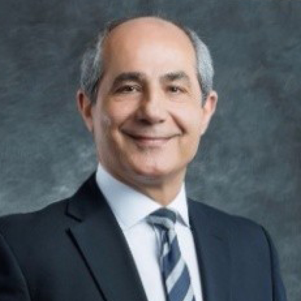
Laith Altimime
President, Semi Europe
As President of SEMI Europe, Laith Altimime leads SEMI’s activities in Europe and Middle East and Africa (EMEA). Altimime has P&L responsibility as well as ownership of all Europe region programs and events, including SEMICON Europa.
He is responsible for establishing industry Standards, advocacy, community development, expositions, and programs. He provides support and services to SEMI members worldwide that have supply chain interests in Europe. He manages and nurtures relationships with SEMI members in the region and globally as well as with local association and constituents in industry, government, and academia.
Altimime has over 35 years of international experience in the semiconductor industry. Prior to joining SEMI in 2015, He held senior leadership positions at NEC, KLA-Tencor, Infineon, Altis, Qimonda and imec.
Abstract:
Global industry growth mega trends, headwinds and opportunities for global Private-Public collaborations.
Stefan Finkbeiner
CEO and GM, Bosch Sensortec GmbH
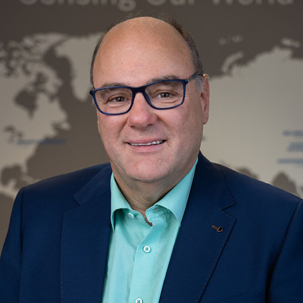
Stefan Finkbeiner
CEO and GM, Bosch Sensortec GmbH
Bio:
Stefan Finkbeiner received his Diploma in Physics from University of Karlsruhe in 1992. He then joined Max-Planck-Institut in Stuttgart and there received his PhD in Physics in 1995.
He joined Robert Bosch GmbH in 1995 and has been working in different positions related to the research, development, manufacturing, and marketing of sensors for more than 20 years. Senior positions at Bosch have included Director of Marketing for sensors, Director of Corporate Research in microsystems technology, and Vice President of Engineering for sensors.
In 2015, Dr. Finkbeiner was awarded with the prestigious lifetime achievement award from the MEMS & Sensors Industry Group.
Abstract:
Tiny sensors are catalysts for addressing major modern challenges: Enhancing air quality and elevating human well-being. Clean air is vital for well-being. Innovative MEMS technology measures health-damaging pollutants in the air and can help improve air quality. To further enhance well-being, MEMS sensors can track full-body motion, coupled with AI-driven personalization, providing real-time qualitative and quantitative feedback to users.
These examples underscore the synergy between MEMS sensors and smart algorithms, unlocking vast potential across diverse fields. This presentation emphasizes the transformative power of MEMS sensors, envisioning a world where technology not only enhances devices but also transforms lives. The presentation concludes with an outlook on innovative use cases ahead.
Theodore Sizer
EVP, Optical Research, Nokia Bell Labs
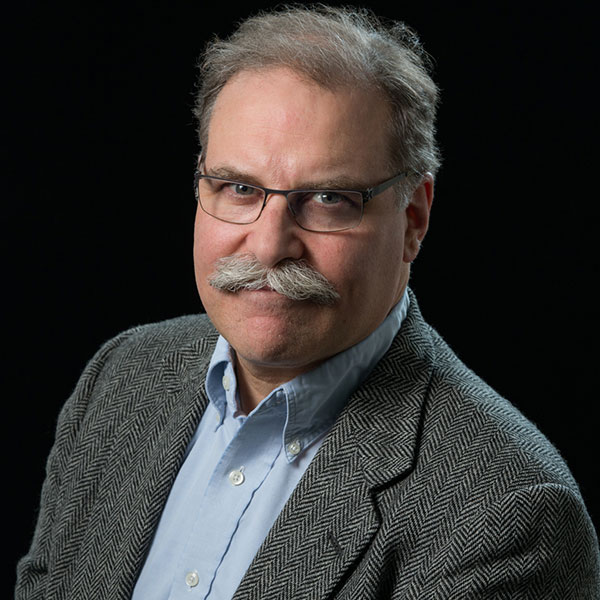
Theodore Sizer
EVP, Optical Research, Nokia Bell Labs
Bio :
Dr. Theodore (Tod) Sizer leads the Optical System and Device Research Lab in Nokia Bell Labs, leading teams innovating in all aspects of optical systems and devices for access, core, submarine, satellite, and data center communications. Prior to his current role, Tod lead Wireless Research in Nokia Bell Labs for eight years driving the vision and research of 5G. Tod graduated from Amherst College, and received his Masters and Doctorate in Optics from the Institute of Optics at the University of Rochester. In 2012 he received the Popular Science Breakthrough Innovation award for the lightRadio invention. Tod is a Fellow of Bell Labs, WWRF, and IEEE. He is the author of 55 US patents and a member of the IEEE and Optica.
Abstract :
Outside of the first 100m which might be carried over WiFi or 5G, nearly all communications are over optical fiber whether it is subsea, terrestrial, fiber to the home, or in the data center. This reality, however, is facing significant challenges due to fundamental limits we have reached in fiber communications. Managing the continued massive growth in communication requires new innovation to overcome the limits with new architectures, systems, and devices. For the optoelectronic semiconductor industry the challenge is to increase speed and parallelism in our devices while reducing the cost and energy per bit carried. In this talk we will share more on the challenge as well as the ways we are addressing in inside Nokia Bell Labs, particularly with research at the III-V Lab joint venture celebrating its 20th anniversary this year.
Fabio Gualandris
President Quality, Manufacturing & Technology, STMicroelectronics
Fabio Gualandris
President Quality, Manufacturing & Technology, STMicroelectronics
Bio :
Fabio is STMicroelectronics’ President, Quality, Manufacturing, and Technology and has held this position since July 2023. He was responsible for the company’s Back-End Manufacturing & Technology organization since 2016 and also led the Company’s Testing Council, alongside its manufacturing strategy in Asia and efforts in System-in-Package technology. Fabio is a member of ST’s Executive Committee.
Fabio joined SGS Microelettronica (now ST) R&D in 1984. He became R&D Director of Operations in 1989 and became Automotive BU Director in 1996. After two years as President and CEO of Semitool, he rejoined ST in 2000 as Group VP responsible for memory products including the RAM/PSRAM and Automotive Flash. In 2005, Fabio was appointed CEO of ST Incard, an ST smart-card subsidiary. In 2008-2010, he served as VP and Supply Chain General Manager at ST’s memory JV with Intel. In 2011, Fabio was appointed ST’s Executive Vice President, Product Quality Excellence.
Fabio has authored several technical and managerial papers and holds multiple international patents. He serves as Chairman of STS, ST's manufacturing JV in China. Fabio was born in Bergamo, Italy, in 1959. He is a Doctor in Physics from the University of Milan.
Abstract :
Since its inception in 1958, semiconductor technology has undergone rapid growth and innovation, positioning itself as one of the most dynamic segments in technological advancement. Following Moore's Law on technology evolution, and then transitioning to "More than Moore" approaches, the technology has progressed towards SoC and SiP architectures, ultimately leading to heterogeneous integration and chiplet technologies. New materials such as SiC and GaN have also been introduced, complementing Silicon, which still remains indisputably the main actor.Alongside these materials, new manufacturing techniques including SOI, W2W bonding, PLP, Fan-In-Fan-Out, DCI, PCM, FD-SOI, and II-VI quantum dots have emerged. The advancement of semiconductor technology moved hand in hand with increasing in volumes, data processing capabilities, and automation, paving the way for Edge AI applications that leverage deep learning and ML algos.
To sustain complexity and innovation, we implement edge-to-edge technology governance with integrated planning, data-driven decisions, and multidimensional organizational structures. Specific examples will clarify these concepts.
Abstract:
Since its inception in 1958, semiconductor technology has undergone rapid growth and innovation, positioning itself as one of the most dynamic segments in technological advancement. Following Moore's Law on technology evolution, and then transitioning to "More than Moore" approaches, the technology has progressed towards SoC and SiP architectures, ultimately leading to heterogeneous integration and chiplet technologies. New materials such as SiC and GaN have also been introduced, complementing Silicon, which still remains indisputably the main actor. Alongside these materials, new manufacturing techniques including SOI, W2W bonding, PLP, Fan-In-Fan-Out, DCI, PCM, FD-SOI, and II-VI quantum dots have emerged. The advancement of semiconductor technology moved hand in hand with increasing in volumes, data processing capabilities, and automation, paving the way for Edge AI applications that leverage deep learning and ML algos.
To sustain complexity and innovation, we implement edge-to-edge technology governance with integrated planning, data-driven decisions, and multidimensional organizational structures. Specific examples will clarify these concepts.
Sanjay Natarajan
SVP & GM, Components Research, Intel
Sanjay Natarajan
SVP & GM, Components Research, Intel
Bio :
Sanjay Natarajan is a Senior Vice President and General Manager of Intel Foundry Technology Research & External R&D Engagements group at Intel Corporation. He is responsible for Intel's internal semiconductor research, external engagements with Universities and Consortia, and government engagements worldwide related to semiconductor R&D. During his 31-year career in the semiconductor R&D industry, Sanjay led the development of Intel's 14nm process technology, and prior to that, he led development of Intel's industry-leading 32nm process technology. In addition to Intel, Sanjay has held senior executive positions at Applied Materials, where he led a group developing new types of semiconductor equipment focused on extending Moore’s Law. Outside of work, Sanjay is a Research Professor in the Department of Mechanical & Materials Engineering at Portland State University. He also serves on the Advisory Boards to the Deans of Engineering at Portland State University and Carnegie Mellon University and serves on the Advisory Council for the National Science Foundation Engineering Directorate. He is an IEEE member and received his BS, MS, PhD in Electrical Engineering from Carnegie Mellon University.
Abstract :
For nearly 60 years, Moore’s Law has exponentially increased our ability to compute and has transformed the way we live. Today we live in a world in which nearly every aspect of our lives is touched by technology, including technology itself - which now finds itself in a virtuous cycle of increasing demand driven by increasing capability.
As graphics and AI applications create new and taxing compute workloads, storage needs and power-hungry data transfer rates, advancing Moore’s Law has become more relevant than ever.
Continued dimensional scaling, additional new materials, novel architectures and disruptive innovation at all levels of the compute system drive Intel’s research on the fundamentals of semiconductor technology in our relentless pursuit of Moore’s Law.
Laura Matz
CSTO, Merck
Laura Matz
CSTO, Merck
Bio :
Dr. Laura Matz serves as the Chief Science and Technology Officer at Merck KGaA Darmstadt, Germany, a role that entails spearheading the innovation agenda of a distinguished science and technology enterprise with a heritage exceeding 350 years in chemistry, biotechnology, and integrated materials solutions.
In her capacity, Laura collaborates closely with the Company Board and partners with Innovation Heads across Merck KGaA's three leading industry verticals: Life Science, Healthcare, and Electronics. Her visionary leadership is instrumental in shaping the future of the enterprise, leveraging digital and AI/ML technologies to drive innovation, exploring new markets, fostering strategic partnerships, and developing cutting-edge capabilities and digital business models to deliver groundbreaking solutions. A recent notable achievement includes her role as CEO in launching Athinia™, a joint venture with Palantir, which introduced a pioneering data collaboration platform for the semiconductor ecosystem.
Prior to assuming the role of CSTO, Laura held the position of Senior Vice President within EMD Electronics, previously Versum Materials and Air Products Electronics division. With over 20 years of experience in semiconductor manufacturing and a decade dedicated to running semiconductor materials businesses, she has been a driving force in advancing semiconductor materials development, emphasizing robust R&D initiatives to fuel business growth.
Laura is well-recognized for her leadership style, fostering diverse teams to innovate and solve complex challenges facing humanity. She advocates for the empowerment of young talent in science and engineering, recognizing their potential to drive meaningful change.
Beyond her role at Merck KGaA, Laura serves on the Board of Directors of transformative organizations. She is a board member of AIChE (American Institute of Chemical Engineers), championing a mission to inspire a safe, connected, and inclusive community of chemical engineering professionals worldwide. She contributes on the Board of SEMI Impact for Skills, a governance program focused on upskilling and reskilling initiatives, talent attraction, and accessing funding opportunities. Laura also serves as Director on the board of AION Labs, a Venture Studio pioneering a novel AI-based paradigm to drug innovation.
With her extensive industry experience, Laura is well regarded as a thought leader at the intersection of science, technology, innovation, and business.
Abstract :
Merck, a leading global Science and Technology company, operates across life science, healthcare, and electronics. With over 350 years ability in chemistry, biotechnology, and integrated materials solutions, Merck is at the forefront of leveraging data and digital technologies to drive innovation. By actively exploring new markets and developing its digital business models, Merck is leveraging its capabilities to deliver groundbreaking solutions to customers and patients.
In this presentation, Laura Matz, Merck's Chief Science and Technology Officer, will discuss the challenges faced by the Healthcare and Semiconductor industries and highlight how Merck utilizes digital business models and tools to provide solutions. Using AI as an example, she will showcase the benefits of data collaboration platforms in both Semiconductor and Healthcare industries as well as how AI is transforming drug discovery for proactive patient care.
Bernhard Quendt
CTO, Thales Group
Bernhard Quendt
CTO, Thales Group
Bio :
Dr. Bernhard Quendt holds engineering degrees from the University of Stuttgart and Télécom Paris (ENST), and completed a PhD at the Technical University of Munich, where he was awarded the Rohde & Schwarz Prize.
Formerly Chief Technical Officer for Siemens Digital Industries, he joined the Siemens Communications division in 1999, before being appointed Vice President, R&D for Siemens Rail Automation in 2005. In 2011, he took charge of platform activities and R&D, as Vice President for Siemens Industrial Automation Systems, and, from 2015, held the position of Chief Technical Officer at Siemens Digital Industries.
Bernhard Quendt joined Thales in 2020 as Chief Technical Officer and Senior Vice President.
Abstract :
Thales is dedicated to build a future we can all trust : Citizens want privacy and trusted Identity, Governments want sovereign supply chains, Airline and Space Operators want long term availability ; all want frugal and energy efficient solutions.
Thales focus on technologies on which we can build upon for the long term and in particular Cybersecurity, Quantum and quantum-proof technologies, Trustable and understandable Artificial Intelligence, Open source Hardware and Software, Compound semiconductors and Advanced Packaging
Partnership is one of the key strategic levers to achieve this goal.
Jean-Philippe Fricker
Chief System Architect and Co-Founder, Cerebras Systems
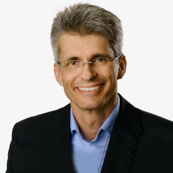
Jean-Philippe Fricker
Chief System Architect and Co-Founder, Cerebras Systems
Bio :
Jean-Philippe (J.P.) is Chief System Architect at Cerebras Systems. Before co-founding Cerebras, J.P. was Senior Hardware Architect at rack-scale flash array startup DSSD (acquired by EMC). Prior to DSSD, J.P. was Lead System Architect at SeaMicro where he designed three generations of fabric-based computer systems. Earlier in his career, J.P. was Director of Hardware Engineering at Alcatel-Lucent and Director of Hardware Engineering at Riverstone Networks. He holds an MS in Electrical Engineering from École Polytechnique Fédérale de Lausanne, Switzerland, and has authored 24 patents.
David Anderson
President, NY CREATES
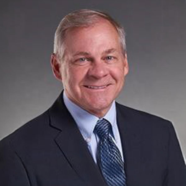
David Anderson
President, NY CREATES
Bio :
A semiconductor industry veteran of 35 years, NY CREATES President David Anderson provides strategic leadership to grow and achieve the organization’s mission of fostering innovation that leads to job creation in New York State. He oversees a program portfolio consisting of 10 sites throughout the state, with expenditures exceeding $350 million annually from industry and state partners, and federal government research and economic development programs.
Previously, David was President of SEMI Americas, leading SEMI’s programs and visibility in the Americas. Before that, he founded and was President and CEO of Novati Technologies, Inc., with the world’s largest portfolio of product development materials. He has held executive positions for development foundries ATDF and SVTC Technologies, and leadership positions at Fairchild Semiconductor, National Semiconductor, the Semiconducto Industry Suppliers Association, and SEMATECH.
David has extensive experience in technology development, process engineering, operations management, supply chain management, international marketing, government relations, and strategy.
Abstract :
This presentation details semiconductor R&D centers as key drivers for stimulating innovation and enhancing chip manufacturing capabilities while bolstering the global semiconductor industry. It will highlight the many unprecedented opportunities for accelerating semiconductor R&D and cultivating a robust ecosystem. Additionally, this presentation showcases the pivotal role of semiconductor R&D centers in harnessing collaborative research efforts, fostering public-private partnerships, and nurturing talent. It will highlight the positive impact of semiconductor R&D centers on industry growth, job creation, and national security. Attendees will gain insights into the innovative research initiatives, cross-sector collaborations, and technology roadmaps that these centers facilitate, and how CHIPS Acts will help to propel the innovations necessary for the future of the semiconductor industry.
Coby Hanoch
CEO, Weebit Nano
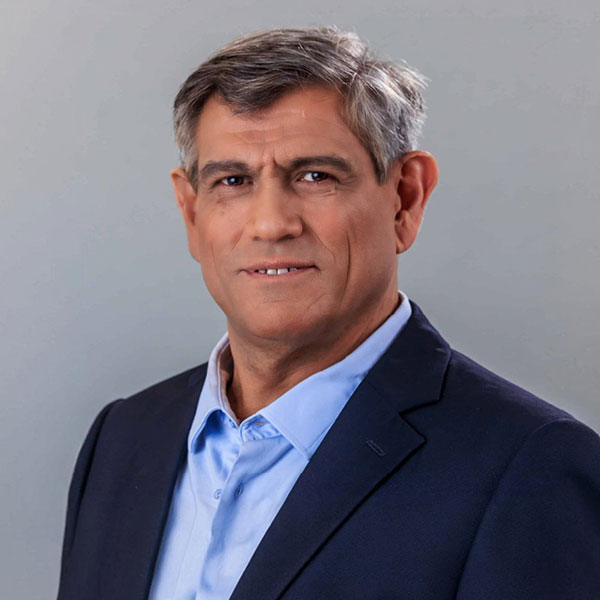
Coby Hanoch
CEO, Weebit Nano
Bio :
Coby is the CEO of Weebit Nano. Coby has nearly 45 years’ of experience in the semiconductor and related industries, including engineering, engineering management, sales, and executive roles. Coby was previously CEO at PacketLight Networks and held VP Worldwide Sales roles at both Verisity and Jasper Design Automation.
Coby also set up his own consulting company, EDAcon Partners, helping startups define their corporate strategies, build their worldwide sales channels, and raise capital. Coby holds a Bachelor of Science in Systems Design from Technion – Israel Institute of Technology.
Emmanuel Sabonnadière
Senior Vice-President for Automotive & Industrial., Soitec
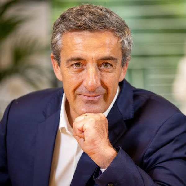
Emmanuel Sabonnadière
Senior Vice-President for Automotive & Industrial., Soitec
Bio:
Since July 2021, Mr. Sabonnadiere has served as the Executive Vice President of the Automotive & Green Industry Division at Soitec, where he also oversees the Strategic Program for Silicon Carbide (SiC).
Prior to this role, from September 2017 to July 2021, Mr. Sabonnadiere held the position of CEO at CEA-Leti, a renowned laboratory in the fields of microelectronics and biotechnology located in Grenoble, France.
Preceding his tenure at CEA-Leti, he served as CEO and Chairman of the Division Professional at Signify, formerly known as Philips Lighting, based in Amsterdam, for two years. From 2014 to 2016, he was a Senior Associate at the MidCap Private Equity firm Gimv, operating out of Paris, Antwerp, Munich, and The Hague. Earlier in his career, Mr. Sabonnadiere held executive roles including CEO and Chairman of General Cable Europe & Africa in Barcelona. He also served as CEO of NKM Noell GmbH, the German branch of the REEL Group, from 2005 to 2008. Furthermore, he spent five years as Vice President of the Distribution Transformers division at Alstom T&D. His career began in 1992 at Schneider Electric, where he held various positions, including Managing Director of equipment units for a decade.
Mr. Sabonnadiere brings with him extensive experience in innovation, technology, and successful business strategies, with a proven track record spanning over three decades. An advocate for operational excellence, technological innovation, talent management, and inspiring leadership, Mr. Sabonnadiere's profound industry experience positions him as a highly respected and knowledgeable Senior actor in the International business landscape.
Mr. Sabonnadiere holds a PhD in Physics and an engineering degree in Information Technology, both from France, as well as an MBA from France.
Abstract:
For the past 30 years, Soitec has been at the forefront of designing and manufacturing semiconductor engineered substrates. As we look ahead, Soitec is positioned to capitalize on markets expected to grow by approximately 20% annually over the coming years, driven by three key megatrends: 5G/6G, Electric Vehicles (EVs), and Artificial Intelligence (AI). We anticipate EVs to emerge as a significant new growth catalyst, aligning with two major trends in the automotive market: the digitalization of vehicles and the electrification of mobility.
By 2030, it is projected that over 45 million cars sold will be EVs. With its enhanced performance in the powertrain, it is estimated that 50% of EVs will integrate Silicon Carbide (SiC) into their power electronics. Soitec's SmartSiC™ engineered substrates represent a new generation of SiC wafers, enhancing the electrical performance and efficiency of power devices, SmartSiC™ offers a greener, faster, and superior solution. It achieves this by reducing CO2 emissions by 70% compared to traditional SiC wafers, accelerating the adoption of 200mm SiC wafers by 2-3 years, and improving device-specific on-resistance by up to 30%. These remarkable capabilities have been possible because of the Pilot Line developed into CEA-Leti, and a reality now through manufacturing in Soitec's new fab, which has been in production since September 2023. The presentation at CEA-Leti 2024 executive session will provide insights into the SmartSiC process and present the latest results on wafers, devices and systems. It will illustrate how SmartSiC™ is driving significant advancements in the SiC business, benefiting both the automotive and Green industry sectors. It will explore the latest developments to be expected at power devices and expected innovations in Automotive & Green Industry
Leroy Liu
CSO, CEO & President’s Office Realtek
Leroy Liu
CSO, CEO & President’s Office Realtek
Bio:
Mr. Liu spans extensively across technology, mergers and acquisitions, and venture capital. Based in Taiwan, Mr. Liu is currently the Chief Strategy Officer at Realtek Semiconductor Corporation. Prior to that Mr. Liu was APAC General Manager with Dialog Semiconductor.
Mr. Liu has bachelor’s and master’s degrees in chemical engineering from the National Taiwan University and is an INSEAD alumni.
Sébastien Dauvé
CEO, CEA-Leti
Sébastien Dauvé
CEO, CEA-Leti
Bio:
Sébastien Dauvé was named CEO of CEA-Leti effective on July 1, 2021, after more than twenty years of experience in microelectronics technologies and their applications, including clean mobility, medicine of the future, cybersecurity, and power electronics.
Sébastien Dauvé started his career at the French Armament Electronics Center, where he worked on developing synthetic-aperture radar. In 2003, he joined CEA-Leti as an industrial transfer manager and supervised several joint research laboratories, in particular with the multinational Michelin.
In 2007, Sébastien Dauvé became a laboratory manager, then head of an R&D department in the area of sensors applied to the Internet of things and electric mobility. During this time, he supported the dissemination of new technologies in industry, including the automotive industry (Renault), aeronautics, national defense (SAFRAN), and microchips with the industry leader Intel. He played an active role in the creation of start-ups in application fields ranging from health to infrastructure security, leading to dozens of new jobs. In 2016, he became Director of the CEA-Leti Systems Division.
From sensors to wireless communication, Sébastien Dauvé has played an active role in the digital transformation, focused on coupling energy frugality and performance. He has made cross-disciplinary approaches central to innovation by harnessing the expertise of talented teams with diverse backgrounds. Their goal is to provide technological tools for meeting the major societal challenges of the future.
Sébastien Dauvé is a graduate of the French Ecole Polytechnique and the National Higher French Institute of Aeronautics and Space (ISAE-SUPAERO).
Michael Tchagaspanian
EVP Strategic Partnership, CEA-Leti
Michael Tchagaspanian
EVP Strategic Partnership, CEA-Leti
Pierre Chastanet
Head of Unit - Microelectronics & Photonics Industry, European Commission
Pierre Chastanet
Head of Unit - Microelectronics & Photonics Industry, European Commission
Bio:
Pierre Chastanet is Head of the Unit for Microelectronics and Photonics Industry at the European Commission, where he manages the development of European semiconductor policy and the implementation of the European Chips Act.
Mr. Chastanet has been working for over 17 years in the European Commission, supervising different digital policies in the areas of cloud, data flows, software, cybersecurity, privacy, green ICT, and telecom innovation.
Prior to that, Mr. Chastanet gained more than 10 years of ICT experience, mostly in various IT management positions in a large multinational company.
He holds a MSc in Telecommunication Engineering from Telecom Paris (Paris Polytechnic Institute), a M.A. in International Politics from the Free University of Brussels (ULB), and a BSc in Economics from the London School of Economics and Political Science. He also earned a Leadership Executive Certificate from Harvard Kennedy School of Government.
Abstract:
With the European Chips Act, the EU will address semiconductor shortages and strengthen Europe’s technological leadership. It will mobilise more than € 43 billion of public and private investments and set measures to prepare, anticipate and swiftly respond to any future supply chain disruptions, together with Member States and our international partners.
This will be achieved based on three pillars of action:
- The "Chips for Europe Initiative" is supporting large-scale technological capacity building and innovation.
- A framework to incentivise public and private investments in manufacturing facilities will ensure the security of supply and resilience of the Union's semiconductor sector.
- A coordination mechanism through the European Semiconductor Board constitutes the key platform for coordination between the Commission, Member States and stakeholders.
The European Chips Act will bolster Europe’s competitiveness and resilience in semiconductor technologies and applications, and strengthen Europe’s technological leadership in the field.
Electronics & Sustainability
Léa Di Cioccio
Eco-Innovation Program Manager, CEA-Leti
Léa Di Cioccio
Eco-Innovation Program Manager, CEA-Leti
Léa Di Cioccio is Director of Research at CEA-Leti. She is currently in charge of the CEA-Leti Eco innovation program.
Since 1990, when she joined the organization, she has conducted research activities in materials, epitaxy, direct bonding, etc. in the fields of 3D integration and power components in the frame of collaborations with STmicrolectronics, SOITEC and in lots European projects. She is the author of more than 200 publications, 5 book chapters and 40 patents. Concerned by the socio-ecological transitions underway, she is working to introduce these new paradigms into the organization's research methodologies and strategy.
Laurent Pain
Sustainable Electronics Program Director, CEA-Leti
Laurent Pain
Sustainable Electronics Program Director, CEA-Leti
Bio:
Laurent Pain is graduated from the Ecole Nationale Supérieure de Physique de Grenoble in 1992. He received his Ph D after his work on DUV resists study. He joined CEA-Leti in 1996 to work on infra-red technology, and then came back to STmicroelectronics in 1999 working on 193nm and e-beam lithography technologies.
From 2008 to 2014, Laurent Pain leaded the lithography laboratory of the silicon technology division of CEA-Leti. He was also managing in parallel the industrial consortium IMAGINE dedicated to the development of multibeam lithography with MAPPER lithography BV.
Since July 2014, within the CEA-Leti Silicon Technology Division, he is now in charge of the business and the partnerships developments of the Silicon Technologies Platform Division.
David Medeiros
Ph.D. Senior Director Engineering, CTO Office, Entegris
David Medeiros
Ph.D. Senior Director Engineering, CTO Office, Entegris
Bio:
David Medeiros has over 30 years of industry experience in the semiconductor industry. He is currently the Senior Director of Engineering in the office of the CTO of Entegris, located at the headquarters in Billerica, MA. His primary focus areas are innovation for sustainability and corporate lithography strategy. He serves as the co-chair of the SEMI PFAS Working Group and is an active member of the SIA PFAS Consortium and the SEMI PFAS Initiative. He is also co-lead of the Materials, Equipment, Metrology, and Inspection (MEMI) working group of the American Semiconductor Innovation Coalition (ASIC). David is a part-time instructor at the Gordon Institute at Tufts University in Medford, MA, teaching Engineering Leadership and Ethics. Prior to joining Entegris in 2021, David spent six years at GlobalFoundries in Malta, NY in executive roles in patterning, capital management, and fab-capacity planning, as well as 17 years at IBM in Yorktown Heights, East Fishkill and Albany, NY, in a variety of engineering and management roles, primarily focused on lithography and patterning. He is trained as an organic chemist, starting his career as a research scientist at the Shipley Company and receiving his PhD from the University of Texas in Austin. He is the co-author of more than 50 technical papers and the co-inventor on over 50 issued US patents.
Abstract :
Water is perhaps the most important substance in semiconductor manufacturing beyond silicon. Today’s fabs use enormous volumes of water with exacting specifications for purity. As the industry grows, there is an increasing focus on strategies for minimizing use, reclamation, and other approaches to ensure a sustainable future for the industry, all without compromising quality. This presentation will provide an overview of the challenges facing semiconductor manufacturers and how innovative solutions provide opportunities for navigating a future that is both technology-enabling and environmentally conscious.
Nadine Allemand
PhD, Deputy Director, CITEPA
Nadine Allemand
PhD, Deputy Director, CITEPA
Bio:
Nadine Allemand is deputy director of Citepa since 2011. After a university degree in atmospheric sciences and a PhD in analytical chemistry, she joined Citepa in 1986. She has extensive experience in air pollution and climate issues and policies and measures to reduce emissions, including improving air quality and mitigating climate change. Among other tasks, she leads the technical-scientific secretariat of the "Task Force on Techno-Economic Issues (TFTEI)" of the Air Convention (CLRTAP) of the United Nations Economic Commission for Europe (UNECE) and participates in numerous works within the framework of this Air Convention. She has been responsible of a large number of technical assistance projects such as for the French Ministry for an Ecological Transition for the development of the national strategy to reduce air pollutant emissions (PREPA), or for international projects for different countries such as Serbia and Turkey to help these two countries to develop their plans to combat air pollution
Abstract:
The presentation will give a brief overview of the role of existing EU policies and measures on the reduction of emissions of air pollutants and improvement of air quality. It will present the new policies developed by the EU and explain what the objectives are.
Jean-Marc Girard
CTO & Sr VP. Manuf. Technologies, Air Liquide
Jean-Marc Girard
CTO & Sr VP. Manuf. Technologies, Air Liquide
Bio :
Jean-Marc Girard, Ph.D. is the CTO and Sr. VP of Manufacturing Technologies at Air Liquide Advanced Materials (ALAM), which is a leading supplier of dry deposition materials and low GWP etching gases. Jean-Marc leads ALAM’s R&D in the EU, US and Japan and oversees strategic partnerships with chip makers, equipment companies, and research institutes.
He graduated from Ecole Normale Superieure de Lyon in physical chemistry, and holds a Ph.D. (1994) from CEA - Université Paris-Sud in Plasma Physics. He joined Air Liquide in 1994 and held several positions of growing responsibilities in France and Japan, serving the semiconductor industry.
Abstract :
Fluorinated gases represent up to 80% of a fab's carbon footprint, and as such, harnessing their emission is key for our customers to meet their climate objectives. Among the other actions undertaken around abatement technologies, substitution -or anticipated substitution- of the highest impact gases is making rapid progresses at advanced nodes. However, installed capacity and legacy nodes manufacturing fabs are mildly receptive to process changes and new ways of collaboration must be developed to decrease the barrier to change.
Isabelle Servin
Sustainability Advisor and Eco-Design Engineer, CEA-Leti
Isabelle Servin
Sustainability Advisor and Eco-Design Engineer, CEA-Leti
Bio:
Isabelle SERVIN is a research scientist at CEA-Leti, Grenoble (France). Since 2022, she has joined the eco-innovation program, as sustainability advisor for Technological Silicon Platform. She evaluates the environnemental impacts of processes in clean room through The Life Cycle Assessment (LCA) methodology for IC industry. She has 20 years of experience in the development of lithography processes for microelectronics, both in industry and R&D. She received her PhD on polymer chemistry from University Pierre & Marie Curie (Paris, France) in 1998.
Abstract:
In semiconductor industry, energy efficiency and water management are crucial to reduce the environmental impacts of chips manufacturing.
CEA-Leti will propose ways to improvement energy efficiency both to infrastructure and production equipment.
Additionally, techniques such as water reuse and adoption of advanced technologies for water treatment and purification are currently implemented to reduce water usage in cleanrooms, contributing thus to sustainable management of resources.
François Marty
In charge of Star Monitoring, Team for the Planet
François Marty
In charge of Star Monitoring, Team for the Planet
Bio :
François has been working in the entrepreneurship and energy transition sectors for 10 years. Jack of all trades in a company, he invests in and advise TFTP’s stars, startups contributing to the transition.
Abstract :
Entrepreneurship is a powerful tool to change the world. Embark with Team for the Planet on a transformative journey to massively tackle CO2 emissions while redefining the paradigms of growth.
Elise Chaumat
Research Engineer—Eco-Innovation and LCA, CEA-Leti
Elise Chaumat
Research Engineer—Eco-Innovation and LCA, CEA-Leti
Bio:
Elise Chaumat is Life Cycle Assessment (LCA) and Eco-Design specialist at CEA-Leti. Elise is graduated from CentralSupelec (2020) and Arts & Métiers ParisTech on Change Management and Sustainable Innovation (2020). She works on environmental assessment and the sustainability of Power Electronic systems.
Abstract:
If many environmental impacts arise from electronics, the management of current and future e-waste has become a priority. With only 17% of the 53.6Mt e-waste generated per year being properly collected and recycled, a better management of electronics systems at their end-of-usage is imperative to reduce pollutions and recover part of strategic and scarce material sources. In this context, the EECONE European project aims at reducing e-waste on an European scale. Within the scope of this project, CEA-Leti, in collaboration with other academic and industrial partners, ambitions to develop a solution enabling the design of more circular and sustainable electronic systems. This talk will present a status of the current development of this solution.
Fabien Chêne
Head of Sustainability Business Europe, Schneider Electric
Fabien Chêne
Head of Sustainability Business Europe, Schneider Electric
Bio:
After finishing his studies - Engineer & Master's Innovation & Technology Management - EM Lyon- Fabien has joined Schneider Electric as a Business Development Manager where he has occupied the role of Director & Principal for Energy & Sustainability services before developing the solutions division of Business.
As the Head of Schneider Sustainability Business Europe, Fabien is at the forefront of advancing the company's commitment to sustainability and energy efficiency .
Fabien both crafts and ensures the adequate execution of strategies that aid global companies reduce their environmental impact & achieve their sustainability goals.
Fabien joined Schneider Sustainability Business in 2013 and has occupied diverse roles gaining a well-rounded and thorough understanding of each sector of operations to best lead the business.
Fabien is an expert advisor specializing in climate change strategy & guiding decarbonization efforts, dedicated to assisting Commercial & Industrial client on their path to Energy Efficiency & Electrification .
Abstract:
Minimizing the carbon footprint of the semiconductor industry is a key priority, particularly with scope 3 posing significant challenges. Decarbonizing the entire value chain effectively demands robust partnerships and industry-wide collaboration. Join us in this session to discover how forming the right partnerships can help reduce the carbon footprint of the semiconductor industry as a whole!
Thierry Chevolleau
Head of Etching Laboratory, CEA-Leti
Thierry Chevolleau
Head of Etching Laboratory, CEA-Leti
Bio:
I am currently heading the etching laboratory at CEA-Leti in France. I joined the CEA-Leti as researcher in the patterning department in 2021. I received the Ph. D degree from Nantes University in France in 1998. After three years in Dresden in Germany as researcher (from 1998 to 2001), I got a position as research engineer at LTM (laboratoire des technologies de la microélectronique) from CNRS and Grenoble Alpes university. I was involved in collaborative R&D program between CNRS, CEA-Leti and STMicroelectronics in the field of plasma etching processing until 2012. Then I became the fab manager of the upstream technological platform (PTA) from the Renatech Network before to join CEA-Leti.
Abstract :
Environment, Safety, and Health (ESH) concerns associated with the semiconductor industry will bring to huge R&D efforts to eliminate the utilization of PFAS in patterning processes and hazardous and critical raw material (CRM) additives from wet cleaning solutions.
The presentation will focus on the pathway to rethink the wet chemistries for semiconductor manufacturing thanks to French i-DEMO-CLEAN consortium including STMicroelectronics (Crolles), CEA-Leti and TECHNIC France.
Jérôme Daviot
R&D and Application Director, Deputy General manager, Technic
Jérôme Daviot
R&D and Application Director, Deputy General manager, Technic
Bio:
After participating and leading chemical design programs throughout various industrial ventures, ranging from a Ph.D. on hydroxylamine cleaning to Cu PCMP with EKC Technology, and further enriched by assignments at prominent European RTOs (LETi, IMEC), he transitioned to the role of R&D director for the Strip/Etch/Clean group at Technic. Over the past 14 years, his team's mandate has been to tackle, refine, and optimize innovative wet processes that could effectively address performance, sustainability, and HSE concerns. Utilizing Technic's growing reputation for addressing industrial issues and wet process changes with a holistic approach, in tandem with chip manufacturers' ESG initiatives, allow to accelerate evaluations and acceptance of innovative eco-designed blends. Recent initiatives such as the CLEAN consortium (LETI/STM/Technic) represent significant contributions to fostering a gradual shift in mindset and showing that designing wet processes in a more systemic eco-friendly way can also offer valuable cost of ownership in the long run.
Ilya Zabelinsky
Co-Founder, ISRL
Ilya Zabelinsky
Co-Founder, ISRL
Bio :
Ilya Zabelinsky is a globally recognized Technical Leader with over 25 years of experience in vacuum and gas abatement applications for Semiconductor manufacturing.
Ilya joined Intel in 1996 and developed his career as operational and engineering leader in SubFAB domain supporting Intel's manufacturing technology transitions and capacity expansion projects in Israel and worldwide. In 2022 Ilya retired from Intel on a mission to “bring the Science to SubFAB” through focused R&D of process materials handling downstream from process chambers. Today Ilya is a co-founder of International SubFAB Research Labs (ISRL). Ilya holds a B.Sc in Chemical Engineering from SCE, Israel.
Abstract :
The Semiconductor Industry’s desire for sustainable manufacturing has many challenges associated with process materials handling downstream from process chambers.
We need to bring science to SubFAB. Connect most advanced research teams worldwide to fundamental problems and provide equipment manufacturers and their customers with scientific knowledge and technical infrastructure that will enable development of breakthrough technologies, encourage collaboration and speed up the innovation cadence.
Charlène Descollonges
Engineer & Hydrologist, ENTREPRENEUR
Charlène Descollonges
Engineer & Hydrologist, ENTREPRENEUR
Bio :
She graduated from a double Master's and Engineering degree and currently works as an independent consultant, author and speaker committed to water protection.
She co-founded “Pour une Hydrologie Régenerative” ("For a regenerative hydrology"), an NGO which aims to restore the water cycle within territories in order to improve their resilience to droughts, floods and erosion.
Her first book “L’Eau - Fake or Not", has gained great success since its launch in may 2023 and helps to better understand the global issues related to water. This book has led to the creation of an expert masterclass on the Sator online platform, as well as two TEDx talks and many conferences across France.
Abstract :
Humans have appropriated water to operate his economic system, to such an extent that we have crossed the planetary limits. It is urgent to change our outlook on freshwater. Water management must become collective and democratic. Otherwise it will increase conflicts of use between humans, or even water wars.
To design desirable futures around water, we must approach the issue from another angle and thus avoid the risks of maladaptation. What if we regenerate the water cycle ?
Sahar Al Kamand
Sales Engineer, Hummink
Sahar Al Kamand
Sales Engineer, Hummink
Bio:
Sahar is a Sales Engineer at Hummink, responsible for identifying new business opportunities and collaborating closely with the business development team to facilitate Hummink's global expansion efforts. Her educational background includes a masters degree in Electronics Engineering with a focus on biomedical applications, as well as a master's degree in Biomaterials and Biodevices from the BME International Program in Paris. She has around 4 years of experience in sales and business development within tech companies, including startups.
Abstract:
In the context of modern manufacturing, sustainability is crucial due to the rising demand for electronic products and subsequent electronic waste issues. Traditional printing methods face limitations in resolution and precision, necessitating advanced techniques like High Precision Capillary Printing (HPCaP). Inspired by Atomic Force Microscopy (AFM), HPCaP utilizes capillary forces for precise printing on various substrates, achieving sub-micron resolutions. This method minimizes material usage, accommodates various inks, and is versatile across substrates, including recyclable ones. HPCaP technology enhances repair processes in industries such as displays, electronics, semiconductors, and automotive, contributing to a more resilient and environmentally friendly future amidst the shift towards a circular economy and eco-conscious innovation
Mattias Espanet
Central Facilities Water Program Manager, STMicroelectronics
Mattias Espanet
Central Facilities Water Program Manager, STMicroelectronics
Bio :
More than 20 years as Water treatment Engineer, in charge of UPW production installations and water management on Rousset ST manufacturing site.
Company Water treatment referent since 2017 in charge of Water Treatment Engineers community management and Water saving program.
Since 2022, at Central Facilities level, in charge of Water, Wastewater, Gas and Chemical scope.
Abstract :
The water-saving journey in the semiconductor industry is a multifaceted challenge that requires a combination of technological innovation, process improvements, regulatory compliance, and corporate commitment to sustainability.
Key points to focus on include reducing water consumption through recycling, technological advancements, and process optimization to mitigate environmental impact and ensure sustainable operations.
Tech for Health
Nadège Nief
Deputy Head of Healthcare Division, CEA-Leti
Nadège Nief
Deputy Head of Healthcare Division, CEA-Leti
Bio:
Biotechnology engineer by education, with additional skills in partnerships development, finance and cross functional management, Nadège spent 10 years in the pharmaceutical CDMO industry before joining CEA-Leti Health in 2017 as Deputy Head. CEA-Leti is a world leading Technological Research Institute specialized in microelectronics and information treatment. Its Healthcare division develops disruptive micro & nano technologies and integrated smart devices with a key mission to create innovation and to transfert it to industrials partners (and/or to create start ups) in the fields of medtech, biotechnology & bioproduction, and environmental monitoring.
Aurore Lepecq
Deputy Head of Energy Electronics & Sensors Systems Department in System Division, CEA-Leti
Aurore Lepecq
Deputy Head of Energy Electronics & Sensors Systems Department in System Division, CEA-Leti
Bio:
With a degree in Physical Sciences and an engineering background, I spent the first 14 years of my career at ST Microelectronics, a worldwild company, where I contributed to several projects in the areas of electronics, microelectronics, and optics. In 2019, I joined CEA--Leti in Grenoble as a Laboratory Manager in the field of Health Technologies (Medical Devices). Since 2023, I'm Deputy Head of the Sensors Systems and Electronic for Energy department at CEA-Leti. The department develop innovative systems that are both high-performing and sustainable. Our services primarily concentrate on three areas: autonomy of sensor systems, power conversion based on wide bandgap transistors, and predictive maintenance of systems.
Philippe Andreucci
Co-Founder, CEO & Member Board of Directors, Injectpower
Selim Olcum
VP of Engineering, Travera
Selim Olcum
VP of Engineering, Travera
Bio :
Dr. Olcum is a co-founder of Travera, a pioneering biotechnology company in functional precision medicine in cancer. He is one of the inventors of Travera’s 2-day Rapid Therapy Guidance Test that measures the ex vivo growth response of live tumor cells to treatment. Dr. Olcum, earned his Ph.D. degree in electrical engineering from Bilkent University. He has completed his post-doctoral training in Biological Engineering at MIT and served as a research scientist at the Koch Institute for Integrative Cancer Research. He is a Ph.D. technologist, has co-authored over 50 papers, is an inventor of 15 issued and pending patents in bioinstrumentation, medical devices, microfluidics, sensors, micro-devices, and their biotechnology and healthcare applications.
Abstract :
Functional precision medicine offers a promising complement to genomics-based cancer therapy guidance by directly testing drug efficacy on patient tumor cells. Travera's test, delivering therapy guidance in just two days, boasts over 80% predictive accuracy across multiple cancers, tissue types and therapies. This talk details Travera's methodology, which integrates single-cell mass measurements with linked brightfield imaging, and discusses linked single-cell volume, density, and morphology and their utilization for improving the predictive accuracy and in broader single-cell data landscape.
Christine Dufour
Silicon Microfluidics Program Manager, X-FAB
Christine Dufour
Silicon Microfluidics Program Manager, X-FAB
Bio :
I have more than 25 years of experience in the CMOS semiconductor industry, working for Philips Semiconductors, NXP and Altis Semiconductor, developing Process Design Kits for RF applications. In 2016, I joined Coventor to lead the development of design flow of PDK and for MEMS designs on the Coventor tool platform. In 2019, I left the design/ software related activities to switch to the manufacturing side. I joined the XFAB BU Microsystems 5 years ago as program manager for the Microfluidic applications. My role is to collaborate closely with our biomedical customers to understand their challenges, identify and devise customized solutions that drive their projects forward. I really enjoy working on cutting edge microsystems for applications such as DNA synthesis, DNA sequencing, cells monitoring and lab-on-chip technologies.
Kalyan Handique
Chief Innovation Officer, CDG, Bio-Rad Laboratories
Kalyan Handique
Chief Innovation Officer, CDG, Bio-Rad Laboratories
Bio:
Dr. Kalyan Handique is one of the most prolific biotech and medical device innovators from Michigan with over 400 world wide patents. He is the founder of two successful healthcare start-ups Handylab and Celsee Inc. He currently serves as the Chief Innovation Officer,CDG at BioRad Laboratories, a leader in global life sciences and clinical diagnostics markets. Kalyan joined BioRad through the successful acquisition of Celsee in April 2020. Celsee focused on developing innovative tehnologies for rare cell and single cell analysis. Before Celsee, Handy was a founder of HandyLab, a molecular diagnostics startup based in Ann Arbor, MI that was sold to Becton Dickinson for $300M+ in late 2009. He serves as an advisor, mentor and board member to many startups and seed funds in the Michigan Biotech Region. Handy holds a PhD in Chemical Engineering from the University of Michigan.
Abstract :
Microfluidics has been at the core of numerous molecular diagnostic tests developed for the research and clinical markets over the past few decades. This technology has enabled the development of portable integrated instruments that can analyze a few biomarkers, such as DNA, RNA, or proteins. These instruments are now available for use at the point of care. However, analyzing multiple biomarkers simultaneously using technologies such as next-gen sequencing comes with its own set of challenges. Interrogation of hundreds to thousands of biomarkers requires complicated sample preparation steps and is cost-prohibitive to run in decentralized settings. New approaches for further miniaturization of sample prep technologies and advanced manufacturing methods are still needed to harness the true power of molecular diagnostics. Advances in microfluidic technology may be the answer.
Enrico Alessi
R&D Manager, STMicroelectronics
Enrico Alessi
R&D Manager, STMicroelectronics
Bio :
After graduating from the University of Catania (Italy) in 1997 with a degree in Electronics Engineering, Enrico's professional career started with IBM and Wind Telecommunications working on ICT and telecommunication standards. In 2000 he joined ST to work on sensors for smart applications and later in the medical segment as R&D Manager and led a strategic project focused on human DNA analysis. During this time, he worked on building semiconductor chips and hybrid silicon-plastic devices, hardware, software and instrumentation for In Vitro Diagnostics, maturing experience in design for manufacturing, technical standards and medical certifications. Today, Enrico is contributing ST to develop the next wave of devices for vital signs monitoring. Focusing on both integrated and system-in-package solutions, he and his team are working on developing devices and methods, platforms and solutions for monitoring vital signs and human physiological parameters for transversal applications from medical field to mobile phones and wearable devices for virtual and augmented reality. Enrico holds a second degree in Computer Science at the University of Catania in 2006.
Abstract :
Vital signs monitoring (VSM) technologies are of great benefit for human life since they can predict heart failures, organs and tissues malfunctions, and metabolic pathways disorders. They represent a convergence of technological advances in materials science, sensors, biosensors, electronics, microfluidic, and artificial intelligence. In this context ST is developing next wave of devices for VSM focusing on integrated and system-in-package solutions, modules and platforms for monitoring physiological parameters targeting transversal applications from medical to consumer fields.
Abdelmadjid Hihi
Deputy Director—Clinical Innovation, CEA-Leti
Abdelmadjid Hihi
Deputy Director—Clinical Innovation, CEA-Leti
Bio :
Dr. Abdelmadjid Hihi is Deputy Director for clinical innovation at DTIS, CEA-Leti’s innovative health technologies division. He is a member of CEA-Leti’s Internal Scientific Council, and is responsible for coordinating international public-private partnerships funded by the European Commission and DARPA in particular for medical devices, biomedical research, and neurotechnologies. Before joining Leti, Madjid was at Génome Québec as Scientific Program Manager; and at Chronogen Inc. (Montreal, Quebec) as R&D group leader. Madjid holds a Ph.D in biological sciences from Lausanne University (1999). He is a former Swiss National Fund postdoctoral fellow, and a McGill University postgraduate alumni.
Abstract :
Integrated medical device development platforms are a must to facilitate the connection between technology R&D and clinical deployment of innovative medical devices. In addition to clinical operability, such platforms may ensure an early compliance to industrial norms and regulatory constraints. These elements are key to successfully bring novel medical devices to the real world. Examples will be discussed based on Leti's cuting-edge research with a focus on brain-computer interfaces to compensate motor handicap, as well as on non-pharmacological therapies for neurodegenerative diseases based on photobiomodulation.
Beatriz Matesanz
MIS Innovation and IrixX Business Segment Director, Thales
Beatriz Matesanz
MIS Innovation and IrixX Business Segment Director, Thales
Bio:
A graduate in industrial and mechanical engineering from the National Institute of Applied Sciences (INSA) in Lyon, France, Beatriz Matesanz Garcia has held various positions at General Electric and then at Thales in strategy, marketing, innovation and sales.
She is currently Innovation Director of the Microwave and Imaging Solutions product line and Director of the IrixX segment, which develops imaging solutions for mobile medical radiology and airport security.
Mykhailo Zarudniev
Research Engineer, CEA-Leti
Mykhailo Zarudniev
Research Engineer, CEA-Leti
Bio:
M. Zarudniev received B.S. (2006) and M.S. (2008) degrees in Space and Aeronautical Systems from the National Technical University of Ukraine, Kyiv Polytechnic Institute, Ukraine, successfully accomplished 3rd year cursus in R&D at Ecole Centrale de Lyon (2009), France, and the Ph.D. (2013) delivered by Lyon University Claude Bernard (France). He joined CEA-LETI (France) in 2012 participating in numerous industrial and collaborative R&D projects working on the multi-sensor dynamical systems for operational awareness and obstacle avoidance. In 2014-2018 the research activity was performed on the embedded signal processing integrated to IR-UWB and FMCW radar sensors. From 2019, he is in charge of the innovative RFIC architectures development for radar and spectral sensing applications.
Abstract :
This presentation spans the latest developments of CEA-LETI in the matter of mmW Radar integrated circuit solutions for vital sign measurements, main features of the mmW radar for this application and perspectives for RF sensors in the near future regarding new opening markets.
Abstract:
This presentation spans the latest developments of CEA-LETI in the matter of mmW Radar integrated circuit solutions for vital sign measurements, main features of the mmW radar for this application and perspectives for RF sensors in the near future regarding new opening markets.
Chiara Paviolo
Research Engineer & Project Leader, CEA-Leti
Chiara Paviolo
Research Engineer & Project Leader, CEA-Leti
Bio :
Chiara Paviolo is a project leader at CEA, working at the interface of engineering, physics and biology. After a PhD in biomedical engineering and a first PostDoc in Australia, she moved to Bordeaux (France) as a Marie-Curie fellow. In 2021 she joined CEA as an R&D engineer on novel microscopy techniques coupled with neural networks. Chiara is now the scientific coordinator of different academic and industrial projects and responsible of the 3D optical imaging development in the laboratory of ‘’Optical instrumentation and data-processing for in vitro imaging’.
Abstract :
To obtain evidence of the processes underlying cancer, we have developed a novel microscope where hardware and software are seamlessly integrated, and uses computational neural networks to determine the evolution of cell phenotypes. The software relies heavily on the use of neural networks for image formation, cell analysis, cell fate prediction and decision making to i) image and analyse in quasi real-time, cell behaviours of thousands of cells in parallel ii) identify variations in cell-state indicative of disease origin, iii) pinpoint the location of the cell of interest and the hardware will allow it to iv) pick-up cells for bio-analysis as a final step. While the live cell imaging will provide information about the past of the cell, the molecular analysis would reflect the present biological state of the cell and the prediction algorithm would then suggest the future state of the cell. The framework we propose is disruptive - we imagine a future where live cell microscopy and biomolecular analysis will form a continuum to generate a comprehensive biological timestamp for any cell of interest.
Abstract:
To obtain evidence of the processes underlying cancer, we have developed a novel microscope where hardware and software are seamlessly integrated, and uses computational neural networks to determine the evolution of cell phenotypes. The software relies heavily on the use of neural networks for image formation, cell analysis, cell fate prediction and decision making to i) image and analyse in quasi real-time, cell behaviours of thousands of cells in parallel ii) identify variations in cell-state indicative of disease origin, iii) pinpoint the location of the cell of interest and the hardware will allow it to iv) pick-up cells for bio-analysis as a final step. While the live cell imaging will provide information about the past of the cell, the molecular analysis would reflect the present biological state of the cell and the prediction algorithm would then suggest the future state of the cell. The framework we propose is disruptive - we imagine a future where live cell microscopy and biomolecular analysis will form a continuum to generate a comprehensive biological timestamp for any cell of interest.
Tristan Caroff
Project Manager on Sensor Systems, CEA-Leti
Tristan Caroff
Project Manager on Sensor Systems, CEA-Leti
Bio:
Dr Tristan CAROFF is a project manager on sensor systems.
After completing his PhD on high temperature superconductor cables in 2008 at Grenoble INP, he joined CEA/LITEN as R&D engineer on thermoelectric systems design for energy harvesting and cooling application.
In 2015, he joined CEA/LETI as project manager on autonomous and low power sensor systems in many field of applications such as oil & gas, predictive maintenance for industry, subsea, ….
Today, his main activities are related to autonomous sensor systems for health and sport applications.
Alexandre Delalleau
Medical Device Platform Manager, CEA-Leti
Alexandre Delalleau
Medical Device Platform Manager, CEA-Leti
Bio :
Alexandre Delalleau achieved an engineering degree in mechanical engineering, a master's degree in numerical modeling, and a doctorate in biomechanics. He is the author of 22 peer-reviewed papers and 4 patents (h-index 10). After starting his career in the MedTech environment at Pierre Fabre Laboratories, he was involved in the founding of the Pixience start-up, which focuses on developing new imaging technologies and software for skin cancer diagnosis. After 8 years as COO and CTO, and successfully launching a CE-marked product on the market, he joined the CEA to manage the Medical Devices Platform. This platform focuses on supporting teams with regulatory issues and technology maturation for clinical trial assessment in accordance with European regulations. More recently, he was appointed to the position of Head of the Quality Regulatory Affairs & Eco-innovation Unit of the CEA-LETI Health Department, where he is responsible for setting up a technological environment compliant with the well-known ISO 13485 standard for MedTech developments.
Jean-Pierre Burnouf
European Ecosystem & Scientific Relations Manager, Sanofi
3D Heterogeneous Integration
Sylvie Joly
Partnerships Manager 3D integration & Packaging, CEA-Leti
Sylvie Joly
Partnerships Manager 3D integration & Packaging, CEA-Leti
BIO:
Sylvie Joly is currently working as 3D integration and packaging Partnerships Manager at CEA-Leti. Sylvie received M.Sc. in Microelectronics from ISEP "Institut Supérieur d'Electronique de Paris" in 1989. She completed her education with a Master in Marketing and Innovation at the Grenoble Ecole de Management (GEM) in 2001. Prior to this position, she worked for more than 8 years as display business developer at CEA-Leti. In 2004 as Sr. Marketing Engineer in the CEA's Technology Transfer Department, she built a strong experience in setting up and managing technical marketing surveys. Before joining CEA, she spent 10 years in the industry as an R&D engineer, and 8 years as Sales engineer in several companies including Hewlett Packard and Ericsson.
Pascal Vivet
Scientific Director, CEA-List
Pascal Vivet
Scientific Director, CEA-List
Bio:
Pascal Vivet is Scientific Director of the Digital Systems and Integrated Circuits Division in CEA-List, Grenoble, France, and co-director of the IRT Nanoelec Smart Imager program. He received his PhD from Grenoble Polytechnical Institute in 2001, designing an asynchronous microprocessor. After 4 years within STMicroelectronics, he joined CEA-Leti in 2003 in the digital design lab. His research interests covers wide aspects of circuit and system level design, ranging from system integration, multi-core architecture, Network-on-Chip, energy efficient design, related CAD design aspects, and in strong links with advanced technologies such as 3D integration, Non-Volatile-Memories, photonics. He was project leader on 3D circuit design and integration since 2011. He participates to various TPC such as ASYNC, DATE, 3DIC, ISLPED conferences. He served as a member of the organizing committee of the 3D workshops series at DATE from 2013 to 2015, and to the D43D workshops since 2011, and to the 3DIC conference. He has authored and co-authored more than 120 papers and holds several patents in the field of digital design. He is member of IEEE.
Jean-Philippe Fricker
Chief System Architect and Co-Founder, Cerebras Systems

Jean-Philippe Fricker
Chief System Architect and Co-Founder, Cerebras Systems
Bio :
Jean-Philippe (J.P.) is Chief System Architect at Cerebras Systems. Before co-founding Cerebras, J.P. was Senior Hardware Architect at rack-scale flash array startup DSSD (acquired by EMC). Prior to DSSD, J.P. was Lead System Architect at SeaMicro where he designed three generations of fabric-based computer systems. Earlier in his career, J.P. was Director of Hardware Engineering at Alcatel-Lucent and Director of Hardware Engineering at Riverstone Networks. He holds an MS in Electrical Engineering from École Polytechnique Fédérale de Lausanne, Switzerland, and has authored 24 patents.
Denis Dutoit
Program Manager, CEA-List
Denis Dutoit
Program Manager, CEA-List
Bio:
Denis Dutoit is senior program manager for advanced computing and digital architectures at CEA-List. He coordinated the European ExaNoDe project that developed a computer node demonstrator combining chiplets, an active interposer, and bare dies in a System-in-Package (SiP). He has also contributed to the architecture of the European Processor Initiative (EPI). His current focus is on architecture pathfinding into chiplet-based designs for computing applications including High Performance Computing, automotive electronics and space components. Before joining CEA, he was a system-on-chip architect at ST Microelectronics and ST Ericsson. He has authored or coauthored more than 20 articles, including invited talks and tutorials at IEEE conferences.
Abstract:
Automotive E/E architecture is going towards centralized computing platforms running a rich set of compute intensive
applications with an increased number of sensors with high data traffic for fusion. Such a computing architecture requires
scalability to cover the needs of all vehicle platforms with a reasonable power consumption and cost. Either software
solutions optimized for flexibility or specialized ASIC solutions optimized for cost and power are not fully satisfactory to
answer centralized automotive platforms. This presentation will show how chiplet-based architectures combined with a
model-based design flow for architecture exploration could answer automotive needs.
Jean Charbonnier
Expert in 3D Integration, CEA-Leti
Jean Charbonnier
Expert in 3D Integration, CEA-Leti
Bio :
Jean Charbonnier, is graduated from National School of Physics of Grenoble in 2001 and obtained his Phd degree in crystallography from University Joseph Fourier of Grenoble in 2006. He joined the 3D wafer level packaging group of CEA-Leti in 2008. He has been working for more than 15 years in Through silicon vias, 3D interconnections and silicon interposers technology. His research interests include High Performance computing, Silicon Photonics Interposer as well as cryo-packaging for Quantum architecture applications. He is currently in charge of coordinating the High Density 3D Integration group within the 3D Integration Technologies Laboratory of CEA-Leti.
Abstract :
Due to the increasing costs of advanced nodes and the difficulties of shrinking analog and circuit input-output signals (IOs), alternatives to single die architectures are becoming mainstream. Scalable modular architectures and function partitioning paves the way for new system approaches using 3D technologies. 3D interconnects offers a breakthrough in terms of density, bandwidth, and limit overall power consumption. CEA-Leti’s advanced heterogeneous packaging research leverages expertise in 3D integration by means of Through Silicon Via (TSV) and Hybrid Bonding (HB) technologies developments since more than 15 years. This presentation will exposed the synergy of these key enablers through two meaningful examples for edge IA sensors and HPC applications.
Emilie Bourjot
Project Manager in 3D & BEOL Integration, CEA-Leti
Emilie Bourjot
Project Manager in 3D & BEOL Integration, CEA-Leti
Bio:
Emilie Bourjot is Project Manager and responsible of hybrid bonding integration team in 3D & packaging laboratory at CEA-Leti since 2018. Her current activities involve developing advanced hybrid bonding schemes for 3D integration in wafer to wafer and die to wafer approaches. Prior to joining CEA-Leti, she worked within Microelectronics foundries and R&D centers on the development of advanced FDSOI technologies and sub-3nm nodes. Her area of expertise includes contact, BEOL and hybrid bonding integration.
Abstract :
Due to the increasing costs of advanced nodes and the difficulties of shrinking analog and circuit input-output signals (IOs), alternatives to single die architectures are becoming mainstream. Scalable modular architectures and function partitioning paves the way for new system approaches using 3D technologies. 3D interconnects offers a breakthrough in terms of density, bandwidth, and limit overall power consumption. CEA-Leti’s advanced heterogeneous packaging research leverages expertise in 3D integration by means of Through Silicon Via (TSV) and Hybrid Bonding (HB) technologies developments since more than 15 years. This presentation will exposed the synergy of these key enablers through two meaningful examples for edge IA sensors and HPC applications.
Due to the increasing costs of advanced nodes and the difficulties of shrinking analog and circuit input-output signals (IOs), alternatives to single die architectures are becoming mainstream. Scalable modular architectures and function partitioning paves the way for new system approaches using 3D technologies. 3D interconnects offers a breakthrough in terms of density, bandwidth, and limit overall power consumption. CEA-Leti’s advanced heterogeneous packaging research leverages expertise in 3D integration by means of Through Silicon Via (TSV) and Hybrid Bonding (HB) technologies developments since more than 15 years. This presentation will exposed the synergy of these key enablers through two meaningful examples for edge IA sensors and HPC applications.
Heiko Dudek
Technical Account Manager, 3D-IC & Heterogeneous IC Packaging, Siemens EDA
Heiko Dudek
Technical Account Manager, 3D-IC & Heterogeneous IC Packaging, Siemens EDA
Bio:
Heiko Dudek joined Siemens in 2021, M.Sc. Electrical Engineering, 26 years in EDA in various positions, including application engineering, R&D, services and technical sales, looking after solutions around advanced IC Packaging and signal and power integrity analysis.
Michael Campbell
Senior Engineer—Collaboration Spokesperson, CERN
Michael Campbell
Senior Engineer—Collaboration Spokesperson, CERN
Bio:
Michael Campbell is a senior engineer at CERN. He is spokesperson of the Medipix Collaborations which seek to disseminate pixel detector technology from High Energy Physics to many different fields. The work of the Collaborations has enabled new approaches in diverse domains ranging from dosimetry in space to radiation detection in classrooms and from industrial X-ray applications all the way through to spectroscopic medical X-ray imaging. The Collaborations have also pioneered the development of high granularity timing detectors used both at CERN experiments and in various quantum imaging applications.
Abstract:
We have developed large area ASIC's which can be processed with Through Silicon Vias and combined with an appropriate sensor to cover a large sensitive area seamlessly. The presentation will focus on the ASIC design and how we approached the challenge of creating a device which can be tiled on 4 sides. We will report on recent progress in constructing a large area device.
Séverine Cheramy
Product Line Manager, Aledia
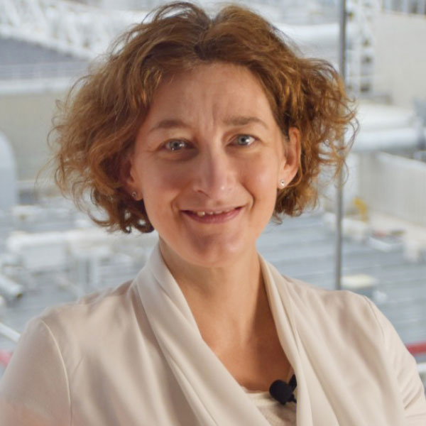
Séverine Cheramy
Product Line Manager, Aledia
Bio:
Séverine Chéramy holds an engineering degree having specialized in material science.
She has spent over eight years at GEMALTO, a leading smart-card company developing technologies for secure solutions such as contactless smart cards & electronic passports.
In 2008, she joined CEA-Leti and for 11 years occupied various roles related to semiconductor 3D integration, as project and team leader,.In January 2017, she took the responsibility for 3D integration strategy and related business development. She was also director of the 3D project of ITR (Institute of Technological Research) Nanoelec from 2012 to 2020.
In 2021, she joined ALEDIA, spin-off of CEA-Leti, as product line manager for Smart-Pixel line. She coordinates the products life from specification to commercialization and manages the roadmap , matching customers’ needs and production’s requirements.
Abstract :
Aledia has developed a unique GaN-on-Silicon 3D µLED technology enabling the use of standard large-area silicon wafers. This cost-effective technology combines the interest of high manufacturability together with easy integration of electronics, and therefore enables access to completely new display formats based on µLEDs.
The talk will focus on heterogeneous integrations developped at Aledia which combine the emission function and the CMOS driver.
Romain Coffy
Packaging Engineer, STMicroelectronics
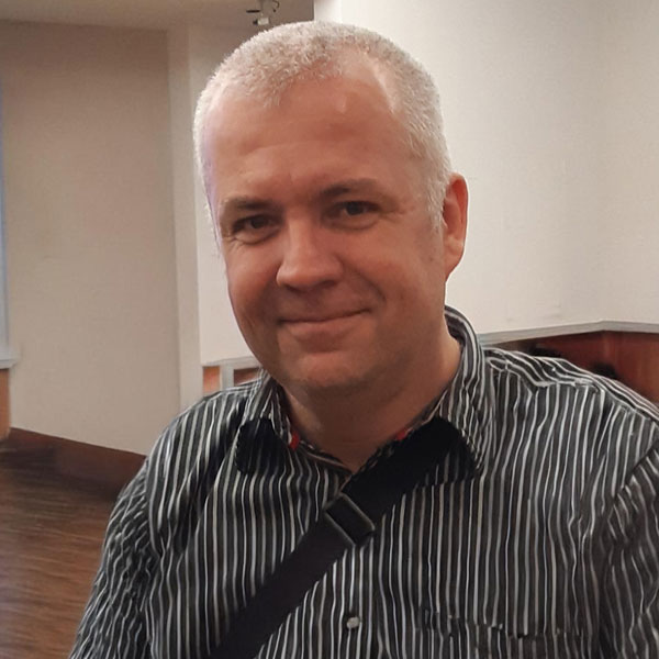
Romain Coffy
Packaging Engineer, STMicroelectronics
Bio :
Romain Coffy is a packaging engineer at STMicroelectronics based in Grenoble, where he is in charge of packaging innovation and networking within the Back-End Manufacturing & Technology group.
His main responsibilities encompass supporting the development of new innovative technological solutions, overseeing the technical roadmap for ST's entire packaging team, supporting market analysis activity, fostering relationships with labs and universities, assisting with patenting activities, and advancing sustainability initiatives.
With over 20 years of experience, Romain is the author of numerous patents in the packaging field.
He earned his Engineering degree from the “École Nationale Supérieure de Physique de Grenoble” (INPG) in 2002.
Frederic Devriere
Collaborative R&D Manager, Teledyne e2v
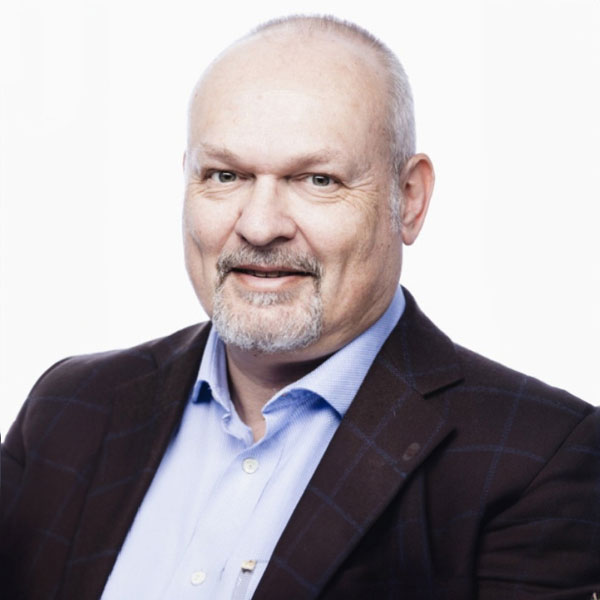
Frederic Devriere
Collaborative R&D Manager, Teledyne e2v
Bio :
Frederic Devriere is responsible at Teledyne e2v for the collaborative projects, and public affairs.
After 15 years of technical positions at Alcatel or Philips, were he was successively electronics or asic designers, then project manager, he joined Teledyne e2v (at that time Atmel), in 2003.
He occupied various roles, from which product manager and strategic marketing manager.
he is graduated from Ecole Supérieure d'Electricité in France in 1992.
Abstract :
Assembly capabilities for low and medium volumes
Teledyne e2v is leading one of the 68 projects of the IPCEI ME/CT, with the aim to develop assembly capabilities for small and medium volumes. This will benefit to the whole ecosystem, who has now an european source for high reliabilty advanced packaging, including System-in-package and flip-chip on organic substrates.
Jean-Stéphane Mottet
Technical Product & Sales Manager, SET

Dale McHerron
Chief Strategist, Chiplets & Advanced Packaging, IBM Research
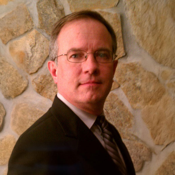
Dale McHerron
Chief Strategist, Chiplets & Advanced Packaging, IBM Research
Bio :
Dale is currently the Chief Strategist for IBM Research Chiplet and Advanced Packaging Group based in Albany, New York. Prior to his current role, Dale was Senior Manager and Senior Technical Staff Member at IBM Research with responsibility for developing and leading IBM’s Heterogeneous Integration Research Program and principal investigator in the IBM AI Hardware Research Center. Over his 30 + year career at IBM, Dale has held various technical, managerial, and business development positions in both advanced packaging and CMOS logic R&D. Dale received his PhD in Chemical Engineering from Virginia Tech with a focus on polymeric materials. Dale has co authored numerous research papers and holds multiple patents in the field of microelectronics.
Abstract :
High performance computing (HPC) and AI applications are driving capacity and complexity of computational workloads at an ever increasing rate. In order to sustain these trends and improve energy efficiency, new hardware technologies and architectures are required. Silicon scaling and design innovations will not be sufficient to meet this challenge. Innovations in advanced packaging, heterogeneous integration, and chiplet architectures hold great promise to deliver system level performance improvements for these critical workloads and provide energy efficiency improvements for the next decade and beyond. In particular, the ability to package multiple silicon chips with a variety of computational functions and technologies in a small form factor will be critical. Furthermore, these technologies must also deliver significant gains in chip to chip communication bandwidth and latency to realize the system level improvements required to sustain these trends and meet the needs of future applications. This talk will discuss trends in workload requirements for HPC / AI and how innovations in packaging and heterogenous integration can enable new hardware architectures to meet the needs of the future.
Darius Bunandar
Chief Scientist, Lightmatter
Darius Bunandar
Chief Scientist, Lightmatter
Bio:
Darius Bunandar is a co-founder and the Chief Scientist at Lightmatter, where his team is leading the evolution of computing, reducing its impact on our planet, and enabling the next great leaps in human progress through silicon photonics. Prior to founding Lightmatter, he obtained his PhD in physics at MIT studying quantum computation and communication using compact nanophotonic circuits. He previously earned his Bachelor of Science degrees in both Physics and Mechanical Engineering from the University of Texas at Austin.
Abstract:
Lightmatter is combining electronics, photonics, and new algorithms to create the next-generation AI/ML supercomputers. In this talk, I will introduce one of our products: Passage. Passage is a wafer-scale programmable photonic interconnect that uses silicon waveguides to enable heterogeneous chiplets to communicate with unprecedented bandwidth.
Thomas Finateu
VP Sensor, Prophesee
Thomas Finateu
VP Sensor, Prophesee
Bio :
Thomas Finateu received the Master’s degree from the Electrical Engineering School of Bordeaux (ENSEIRB), France, in 2004 and the Ph.D. degree in electrical engineering in 2008. His dissertation was done at STMicroelectronics about, Crolles, France.
In 2008, he joined STMicroelectronics, Belgium as an analog engineer where he pursued his analog and RF work for Bluetooth transmitters mobile products.
In 2011, he joined SoftKinetic in Brussels, Belgium, now Sony DepthSensing Solutions. He has been working on Time Of Flight pixels and sensors as analog designer and project leader.
In 2015, he joined Prophesee, as senior analog designer and project leader. He has been working on bio-inspired pixels and sensors pushing further on-chip integration of analog and digital IPs, deeply involved in the joint development with Sony to mature the technology and make it ready for mass production. He is now VP sensor, with more than 20-year experience in the semiconductor industry and IC design.
Abstract :
After an overview on event-based sensors, upcoming trends regarding application domains will be introduced. It will justify the benefits of 3D integration while highlighting the challenges to face. But technology challenges are fortunately not the only ones, design and architecture challenges are arisen too such as edge-AI, multi-modality, multi-layer, pixel shrink, etc... Triple-layer stack and neural network such as GNNs can fill some of these gaps !
Mate Jenei
Tech Lead,3D integration and wiring, IQM Finland Oy
Mate Jenei
Tech Lead,3D integration and wiring, IQM Finland Oy
Bio :
Máté is currently a tech lead on 3D integration and wiring for IQM Quantum Computers, based in Espoo, Finland. His main focus is on developing and testing novel manufacturing techniques employed in superconducting quantum processors and driving the lab-to-fab transition. Prior to joining IQM, he obtained his doctoral degree in 2019 in engineering physics at Aalto University, Finland, researching cryogenic quantum circuits.
He previously earned his M.Sc. in physics from the University of Szeged, Hungary.
Abstract :
IQM Quantum Computers is a full-stack quantum company creating technologies for large-scale quantum computing. One of the key areas of quantum computing is the manufacturing of extreme low-loss RF devices that serve as part of a quantum processing unit (QPU). Our 200-mm fabrication facility has been established to solve the most critical aspects of improving quantum device performance. Highlighting the development of devices based on superconducting circuits, we present our achievements concerning Josephson junction yield and uniformity, qubit coherence time, and superconducting 3D integration techniques that are essential building blocks of our progress.
Julien Schmitt
Technical leader-Compilation, embedded code & simulation platforms,VSORA

Julien Schmitt
Technical leader-Compilation, embedded code & simulation platforms,VSORA
Bio :
Julien Schmitt began his career as a signal processing engeineer and ASIC designer at DiBcom, a leading fabless startup in mobile TV, acquired by Parrot in 2011. He actively participated in the development of a DSP enabling spftware radio. In 2015 he co-founded VSORA offering a new generation of high-performance DSPs intended for algorithmes requiring high computing capacity as well as artificial intelligence.
Abstract :
VSORA is a French semiconductor manufacture providing very high performance AI chips used for Generative AI, autonomous driving and other hard processing taks.
Generative AI is already a huge market, with the hardware expected to reach $50B in 2024. This application requires chips with huge processing power. Focus today is training but tomorrow focus will be inference. However, this market is broken as the current solutions cannot meet the low latency ad power target requirement measured as a cost of 0.2 cents/query.
Dmitriy Gusev
Project Director, Menta SAS
Dmitriy Gusev
Project Director, Menta SAS
Bio :
Dmitriy is a technologist and leader with deep expertise in semiconductors and software, accumulating over 20 years of engineering experience. His track record spans diverse industries including AI, telecom, storage and finance.
He currently leads the Mosaics project and system architecture efforts at Menta SAS.
Before taking on this role, he established and led the hardware team at Plumerai, where they developed Edge AI accelerators. He co-founded Cloudwave, Paris-based startup, that pioneered the smart storage concept.
He holds a MS in Electrical Engineering from MIPT and is an inventor of 1 patent.
Abstract :
Chiplets are ubiquitous today. However, they are used for large and expensive chips serving computing and HPC markets.
The Mosaics project takes the chiplet approach to embedded, industrial and edge AI domains. We present how to use chiplets for designing system-in-package much quicker and cheaper than traditional monolithic IC.
This innovation will open up new markets. The chiplet approach enables the creation of custom integrated circuits for applications that were previously economically unfeasible.
The presentation covers both technical challenges and building of a support ecosystem.
Sense & Act
Vincent Destefanis
Optical Sensors Industrial Partnership Manager, CEA-Leti
Vincent Destefanis
Optical Sensors Industrial Partnership Manager, CEA-Leti
Bio:
Vincent Destefanis is a Partnership Manager for the Optics and Photonic division of CEA-Leti since 2023. Since 2006, he was successively a R&D engineer, a senior technical expert and a partnership manager, this for various leading-edge photonic and CMOS companies (Lynred, STMicroelectronics and IBM).
He holds Master's and Engineering degrees in Electronics, Physics and Materials Science. During his career, Vincent has been successful in creating long-term value in the CMOS and photonic industries, from various valuable contributions to industrial projects and partnerships.
Vincent is now dedicated to the development of industrial partnerships for the development and tech transfer to industry of beyond the state of the art photonic sensing solutions addressing a wide scope of applications.
Pierre-Damien Berger
MEMS Industrial Partnership Manager, CEA-Leti
Pierre-Damien Berger
MEMS Industrial Partnership Manager, CEA-Leti
Bio:
Pierre Damien Berger is MEMS Industrial Partnerships Manager at CEA LETI.
CEA LETI is a leading MEMS R&D lab working for industry, with more than 150 people working on these topics – world’s largest MEMS R&D institute.
Pierre-Damien was previously the MinaSmart (European Digital Innovation Hub) director at Minalogic. He worked before as CPS European projects manager, Head of Smart Devices Program, Industrial Partnership Manager and VP Business Development & Communication at CEA-Leti.
With more than 25 years of experience, 10 years in industry, 15 years in R&D serving industry, his experience has allowed him to master the right balance between business and innovation - Understand and listen to needs, identify and select innovative solutions, enhance the functions that meet expectations, communicate to radiate.
Stephen Bart
Senior Director of Advanced Technology, TDK
Stephen Bart
Senior Director of Advanced Technology, TDK
Bio:
Dr. Bart received the B.S., M.S., and Ph.D. degrees from the Massachusetts Institute of Technology, Cambridge, Massachusetts. He did his doctoral research with Professors Senturia and Lang on analysis and design of the first microfabricated electrostatic motors and pumps. After his PhD work, Dr. Bart joined Analog Devices, Inc., where he designed the MEMS sensor in the well-known Analog Devices, Inc. ADXL150 family of airbag accelerometers, which has over 500 million sensors in the field. From 1996 to 2002 he held several positions at Coventor, Inc., a developer of physical design tools for MEMS systems. Dr. Bart returned to Analog Devices as a Senior Product Development Leader, working on inertial MEMS sensors for the commercial marketplace. Dr. Bart then joined MKS Instruments to develop high-performance, vacuum absolute-pressure sensors for semiconductor and industrial applications. Today, Dr. Bart leads the Advanced Technology group at TDK, where he is developing advanced gas sensors, ultrasonic and acoustic sensors and advanced machine learning and circuit architectures. Dr. Bart's research interests include the design, modeling, and simulation of complex electromechanical systems and Machine Learning methods for sensor data fusion. Dr. Bart holds 11 patents in the microsystems area.
Abstract:
Sensor technology is becoming increasingly sophisticated, affordable, and ubiquitous. Sensors are becoming the human interface to the digital world and, when combined with machine learning (ML), make systems or devices more aware of what the human is doing, about to do, or has just done. As the variety and capabilities of sensors grow, technology has the opportunity to disappear into the background, assisting everyone to be better connected, track their internal health and well being and their external environment, and be enabled with more leisure time. Finally, sensors can optimize the power we consume with all devices, delivering a great experience at the lowest consumption of resources. I will explore these themes, show examples of developments at TDK, and inspire a future vision of smarter sensors.
Joost van Beek
Head of Process Development & Integration, Philips MEMS foundry
Joost van Beek
Head of Process Development & Integration, Philips MEMS foundry
Bio:
Joost van Beek (1969) has been active in MEMS and Micro Systems technology for over 20 years. During his career, he held scientific positions related to these fields at the Massachusetts Institute of Technology, University of California at Berkeley, Philips Research Laboratories, and NXP Semiconductors. Apart from his extensive research experience, he also had the opportunity at Philips and NXP to gain expertise in MEMS process and product release for large volume manufacturing. At NXP and Philips, he was leading projects on RF-Passives, RF-MEMS, MEMS timing devices, Ultrasound Sensing, and others. Currently, he is a member of the management team of the Philips MEMS Foundry in Eindhoven where he is leading the Process Development & Integration group.
Joost received a MSc degree in Applied Physics from the Technical University Eindhoven, and a PhD degree in Electrical Engineering from the Catholic University Leuven. He is co-author of over 50 scientific papers and holds 25 granted patents.
Abstract:
Philips operates a state-of-the-art 2650 m2 pure-play MEMS Foundry on the High Tech Campus in Eindhoven, the Netherlands. This MEMS Foundry is specialized in medium volume custom MEMS manufacturing. An important focal area is the co-development of manufacturing processes for its bio-medical customers. It is thereby uniquely acting as a European pilot line for emerging medical applications.
This presentation will elaborate several on-going MEMS manufacturing activities for various bio-medical applications, such as cell-sorting, neural probing, micro optical tomography and ultrasound imaging.
Lia Li
CEO & Founder, Zero Point Motion

Lia Li
CEO & Founder, Zero Point Motion
Bio:
Dr. Ying Lia Li (Lia), CEO and Founder of Zero Point Motion, is a trailblazer in chip-scale optical inertial sensors. Recognized with the 2021 Institute of Physics Clifford Paterson Medal, the 2022 Innovate UK Women in Innovation Award and named as Sensors Converge ‘Woman of the Year’ 2023, Lia's groundbreaking work redefines sensing using light. A physics graduate from Imperial College, she earned her Ph.D. at University College London, developing optical sensors with applications in macroscopic quantum state preparation. With a track record of coupling optical resonances to mechanical motion, she achieved displacement sensing over 1000x smaller than a single atom. Post-Ph.D., she secured prestigious fellowships from EPSRC and the Royal Academy of Engineering before founding Zero Point Motion in 2020, raising over £6.3M to date.
Abstract:
Zero Point Motion has been developing optomechanical accelerometers and gyroscopes using standard MPW offerings in micro-electro-mechanical systems (MEMS) and photonic integrated circuit (PIC) platforms. By exploiting the coupling between mechanical motion and the evanescent field of optical resonators, exceptional inertial sensing noise floors are demonstrated. In this talk we present progress in our proof-of-concept devices and how we are tackling challenges on creating a compact and low cost system architecture. We are exploring a number of ways to integrate lasers and detectors, capitalizing on emerging capabilities such as heterogeneous solutions.
Philippe Robert
CEO, iNGage
Philippe Robert
CEO, iNGage
Bio :
Philippe Robert is CEO and co-founder of iNGage, a deeptech startup developing a new generation of high-performance MEMS sensors. He holds a PhD in Microtechnologies and began his career at the startup SILMAG, developing advanced magnetic sensor technologies for data storage, before joining THALES to work on high-end MEMS inertial sensors for aerospace and defense applications.
He joined CEA-Leti in 2001, where he held successive leadership roles, including Head of the MEMS Sensors Laboratory and Head of the Microsystems Department (120+ people), before leading Business Development for Microsystems.
In 2025, he founded iNGage as CEO & CTO, leading corporate strategy, fundraising, and execution.
He has authored over 50 scientific publications and holds more than 60 patents, including more than 20 related to the M&NEMS architecture at the core of iNGage’s innovation.
Marc Sansa Perna
Project Manager, Optomechanical Sensors Expert, CEA-Leti
Marc Sansa Perna
Project Manager, Optomechanical Sensors Expert, CEA-Leti
Bio:
Marc Sansa obtained his Ph.D. degree in electronic engineering from the Universitat Autònoma de Barcelona, Barcelona, Spain, in 2013. He is an expert in microelectromechanical system (MEMS) sensors, RF MEMS and optomechanics, having co-authored over 50 publications and several patents. He is currently a project manager at the Sensors and Actuators Laboratory of CEA-Leti.
Marc Chaigneau
Semiconductors Market Manager, Horiba
Pierre Jallon
Director of Technology & Innovation, eLichens
Pierre Jallon
Director of Technology & Innovation, eLichens
Bio:
Pierre Jallon is the Chief Technology Officer of eLichens. He oversees technology development, new products prototyping and strategic marketing for the gas sensor startup. Prior to joining eLichens, Pierre was working with CEA-Leti -one of the most innovative European research centers– as head of laboratory. He was leading a team specialized on innovative medical devices and wearables development.
Abstract :
According to IEA (International Energy Agency), the “methane is responsible for around 30% of the current rise in global temperature”. Reaching climate neutrality in 2050 and meet the European Green Deal objectives requires to reduce methane emissions and track gas leak on production, processing and distribution sites.
An innovative solution will therefore be presented. This solution is being developed in collaboration by eLichens , CEA-Leti and GRDF and includes the development of an innovative new component.
Cyril Herrier
Manager R&D, Aryballe
Cyril Herrier
Manager R&D, Aryballe
Bio :
Cyril obtained his PhD in Materials Chemistry in 2011. During 8 years of academic research (IS2M Mulhouse, ISCR Rennes, IM2NP Marseille, CEA Grenoble), he acquired a strong expertise in structuration, functionalization, and characterization of surfaces at nanometer scale for applications in microbiotechnologies. He joined Aryballe in 2015 as the first research engineer. He is co-author of 19 international papers and co-inventor of 11 patents families.
Abstract :
Mimicking artificially the sense of smell is a technical and intellectual challenge that drives innovative applications development at Aryballe.
In collaboration with the CEA-Grenoble, Aryballe has developed a selective VOC sensor capable of real-time detection and identification. This breakthrough technology enables the generation of large datasets, which can be analyzed using either simple algorithms or more sophisticated machine learning models.
Solutions embedding this type of versatile gas sensor can adress large spectrum of markets, from environment monitoring to consumer domotic. It stimulate also a lot of expectations for Health and Wellness market.
Christina Strohrmann
Director Advanced Engineering, Bosch Sensortec GmbH
Christina Strohrmann
Director Advanced Engineering, Bosch Sensortec GmbH
Bio :
Dr. Christina Strohrmann holds a PhD in Electrical Engineering from ETH Zurich, Switzerland, and an MSc in Information Technology from the University of Kaiserslautern, Germany. She joined Bosch Sensortec GmbH in 2013 and since then works in R&D for sensors in consumer electronics, namely smartphones, wearables, and hearables. She heads the department for advanced engineering, responsible for product pre-development, system architecture, technology and IP Management.
Abstract :
In 2006, Bosch Sensortec released the world's smallest barometric pressure sensor. Since then, we have expanded our portfolio of environmental sensors by humidity sensors, gas sensors, media-robust sensors, and lately particle sensors. All targeting to improve our daily lives and designed for handheld, battery-powered devices. This presentation will provide an overview on applications, use cases, and technologies.
Andreja Erbes
Director, Technology Scouting and R&D Partnerships, STMicroelectronics
Andreja Erbes
Director, Technology Scouting and R&D Partnerships, STMicroelectronics
Bio :
Andreja Erbes received the M.Eng., M.A., and Ph.D. degrees from the Department of Engineering, University of Cambridge, in 2011, 2014, and 2015, respectively, in electrical and electronic engineering. In 2009, he spent one year abroad at the Massachusetts Institute of Technology (Cambridge-MIT Exchange Program) and took part in an undergraduate-research opportunity program with the Weinstein Research Group, where he worked on novel RF MEMS. Since 2022, he is the Director of Technology Scouting and R&D Partnerships at STMicroelectronics within the Analog, Power & Discrete, MEMS and Sensors group.
Abstract :
Sensors and actuators are at the heart of our interactions with the digital world. These devices, based on micro-electro-mechanical systems (MEMS) technologies and embedded with highly efficient and intelligent processing, are effectively merging the offline and online worlds. This fusion of technology into our daily lives is steering us towards a sustainable 'Onlife' era.
For the past 25 years, STMicroelectronics has been a global leader in MEMS, incorporating sustainability practices into the innovative technologies that are developed. This enables new applications and smarter, more sustainable products for our customers.
Piezoelectric MEMS technologies are an integral part of our sensor and actuator products, addressing the diverse requirements of modern applications. The latest advancements in piezoelectric MEMS technology show how process and design innovations are fueling today's applications and anticipating the needs of the future.
Additionally, STMicroelectronics is positioned to aid early-stage companies in their industrialization journey, helping to expedite their production scale-up for cutting-edge sensors and actuators. STMicroelectronics’s Singapore campus is 'Lab-in-Fab,' an 8-inch (200 mm) facility developed in partnership with the Institute of Microelectronics, offers a unique industrialization framework that supports customers in developing and transitioning their novel concept process technology to high-volume production.
Philippe de Bettignies
Technological Roadmap Manager, Horiba France
Philippe de Bettignies
Technological Roadmap Manager, Horiba France
Bio:
Philippe DE BETTIGNIES is the Advanced Technology Roadmap Manager at HORIBA France, in charge of establishing the directions for Innovation and R&D inside the company for the next 5-10 years to support its growth, and also listening to the progress in public research that would be of interest. He was previously the R&D manager of AFM and Raman microscopy in HORIBA during more than 10 years, and works now inside the Innovation team.
Abstract :
HORIBA France, pioneer in optical instrumentation and measurement systems, is a supplier of OEM solutions and benchtop instruments for both industrial and academic sectors. Targeting markets such as semiconductor metrology, environmental monitoring, and life sciences, HORIBA is developing a new range of optical sensors while scaling up current technologies (Raman, Photoluminescence, Ellipsometry) from laboratory settings to industrial environments.
In this presentation, we will present our roadmap for these advanced sensors, along with innovations in the needed sub-components to address the market challenges such as throughput enhancement, compact design, robustness, and seamless integration within fabrication facilities. We will illustrate the practical application of these developments with the Raman metrology inspection in semiconductor manufacturing.
Abstract:
HORIBA France, pioneer in optical instrumentation and measurement systems, is a supplier of OEM solutions and benchtop instruments for both industrial and academic sectors. Targeting markets such as semiconductor metrology, environmental monitoring, and life sciences, HORIBA is developing a new range of optical sensors while scaling up current technologies (Raman, Photoluminescence, Ellipsometry) from laboratory settings to industrial environments.
In this presentation, we will present our roadmap for these advanced sensors, along with innovations in the needed sub-components to address the market challenges such as throughput enhancement, compact design, robustness, and seamless integration within fabrication facilities. We will illustrate the practical application of these developments with the Raman metrology inspection in semiconductor manufacturing.
New Materials for Computing
François Andrieu
Head of Memory & Computing Laboratory, CEA-Leti
François Andrieu
Head of Memory & Computing Laboratory, CEA-Leti
Dr. François Andrieu is CEA fellow and the head of Laboratory “Nano-devices for Memory and Computing” at CEA-Leti, Grenoble, France.
He has been strongly involved in the development of the Fully-Depleted-Silicon-On-Insulator (FD-SOI) CMOS technology at Leti and with STMicroelectronics, where he was assigned between 2012-2015 in the process-integration and technology-to-design groups. His fields of interest are: NVM Resistive-RAM, In-Memory-Computing, advanced CMOS transistors, 3D-sequential integration.
He is the author or co-author of more than 34 patents, 240 conference abstracts or refereed journal articles, 11 invited papers and 3 book chapters. He received the IEEE senior grade in 2018, the European ERC consolidator grant in 2019 and the IEEE/SEE Brillouin award in 2018.
Philippe Rodriguez
Head of Laboratory, CEA-Leti
Philippe Rodriguez
Head of Laboratory, CEA-Leti
Bio:
Philippe Rodriguez is a research engineer and laboratory manager at CEA-Leti in the Semiconductor Platforms Division.
He received his Ph.D. in 2007 from the University of Lyon 1 in Materials Chemistry for his work on metal organic vapor phase epitaxy growth of B(In)GaAs epilayers. From 2007 to 2009, he worked at the CNRS (French National Center for Scientific Research) developing deposition methods on structured substrates for process intensification applications. In 2009, he started his career at the CEA (French Alternative Energies and Atomic Energy Commission). First, he worked on the coating and fluidization of dense powders by fluidized bed metal-organic chemical vapor deposition for the development of new nuclear fuels (2009 - 2011). Then, he developed silica permeation barriers by magnetron sputtering for laser megajoule gas targets (2011 - 2013). Finally, he joined CEA-Leti in Oct. 2013. His research activity is mainly focused on advanced contact technologies for electronics and photonics applications. He develops contact metallization for advanced CMOS and photonics devices (Si, Ge(Sn), III-V and GaN materials) and also deals with surface preparation and interface modulation prior to metallization. He led the contact team at CEA-Leti between 2017 and 2020 and became head of the Advanced Materials Deposition Laboratory in February 2020. In Sept. 2022, he joined the Surface and Interface Science and Engineering Department and since Jan. 2023, he is in charge of the Laboratory of Wet Surface Preparation, Epitaxy and Thermal Treatment Processes.
He is the author and co-author of approximately 100 peer-reviewed journal articles, 115 international conference papers, 2 book chapters, and 15 patents.
Uygar Avci
Director, Novel Devices and Memory in Foundry Technology Research, Intel
Uygar Avci
Director, Novel Devices and Memory in Foundry Technology Research, Intel
Bio:
Uygar Avci is a Senior Principal Engineer at Intel Corporation and is currently leading Novel Devices and Memory Group in Foundry Technology Research. He is responsible for delivering new transistor and memory devices by bridging Physics-based understanding of new materials and experimental realities to enable viable semiconductor devices with power, performance and scaling benefit. He was an Editor for the IEEE Transactions on Electron Devices and is currently in the Executive Committee of the IEDM Conference. He has over 100 patents and has co-authored more than fifty papers. Uygar received double-major degrees in Physics and Electrical Engineering in Turkey and his PhD degree in Applied Physics from Cornell University.
Abstract :
As the demand for semiconductor technology increases through AI applications and number of electronic devices, improving power efficiency and scaling of the transistor and memory elements is vital. New materials such as Ferroelectrics for memory and TMD materials for logic offer great potential for scaling vs. the state-of-the-art devices and also for lowering power through their intrinsic properties. This talk will demonstrate recent advances in these devices and key challenges the researchers are focusing on.
Salim El Kazzi
2D Product Manager, Aixtron
Salim El Kazzi
2D Product Manager, Aixtron
Bio :
Dr. Salim El Kazzi leads the 2D product management at AIXTRON, the leading provider of deposition equipment of the compound semiconductor industry. In 2012, he received his Ph.D. from IEMN-Lille, France, specializing in III-V growth for their integration on Silicon. He then joined imec in Belgium contributing to the CMOS logic program on III-V and 2D deposition working on both research & industrial equipment. In 2019, he pioneered the 2D activities at Applied Material – NUS Advanced Corporate Laboratory, Singapore, where he explored the use low dimensional materials for both FEOL and BEOL applications.
Abstract :
It is becoming obvious that the need of novel materials is a must to pursue the scaling of IC chips. 2D materials are among the most promising and published materials that not only academics are reporting but also high volume manufacturers. One thing is certain is that issues of reproducibility, yield and repeatable performance need to be urgently addressed for 2D materials to reach industry. In short, like every new material, 2D needs to overcome the strict requirements of Si FABs. As a unique provider of 300 mm 2D tools, we will show how AIXTRON is able to mature 300 mm product solutions to offer 2D volume manufacturing for the IC fabs of tomorrow.
Lucie Le Van Jodin
Research Scientist, CEA-Leti
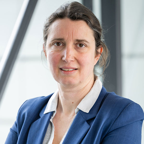
Lucie Le Van Jodin
Research Scientist, CEA-Leti
Bio :
Lucie Le Van-Jodin, Ph.D. is a project manager and a team leader for 2D material transfer at CEA-Leti. Lucie started her scientific carrier studying thermoelectricity during her Ph.D research. She worked at CEA from 2003 on carbon nanotubes for chemtronics, developing growth and characterization of this material. She spent more than 10 years in the CEA’s microbatteries Lab. There, she studied the relationship between the structural and electrical properties of the inorganic electrolyte. In 2018, she joined the film transfer Lab (LIFT). She is working on transfer of various materials as silicon, III-V, piezoelectric, wide gap materials… mainly by SmartCut™ technology. Recently, she focused her works on 2D material transfer for microelectronics applications.
Abstract :
Since the discovery of graphene and more generally of 2D materials, numerous studies have demonstrated the potential of these materials that allow a drastic devices size reduction, performances improvement, low power, new properties… That is why they are seen as the ultimate materials for the microelectronics of the future.. Nowadays, they can be found at several levels, in a wide variety of applications such as transistors, sensors, memories, RF switches...
However, the transition from lab to fab remains challenging. The implementation of 200 and 300 mm characterization capability for 2D materials at CEA enables us to work on this transition to industrial processes. Wafer scale growth, transfer such as integration and van der Waals interfaces preservation are intensively studied since they are key points for the successful manufacturing of industrial 2D materials devices.
Andrea Illiberi
Team Leader, ASM Corporate R&D
Andrea Illiberi
Team Leader, ASM Corporate R&D
Bio:
Andrea is head of the "Active Layers and Exploratory Materials" team at ASM Corporate R&D, based in imec.
Andrea received a Ph.D. in Astrophysics and Plasma Physics from the University of Milano. As post-doctoral researcher at the Eindhoven University of Technology, he worked on plasma based deposition of semiconducting thin films. As Sr. Research Scientist at TNO, he pioneered the development of the Spatial ALD technology for which he received the Paul H. Holloway Young Investigator Award by the American Vacuum Society.
At ASM Andrea works on atomic layer deposition of new dielectric and semiconductive oxides for logic and memory applications.
Abstract:
The architectures of integrated logic and memory devices have shifted from 2D to 3D layouts, enabling a continued scaling of device densities. Atomic layer deposition allows the conformal deposition of thin films with sub-nm thickness control on high aspect ratio 3D structures. ALD has become the technique of choice for the synthesis of an increasing number of materials in advanced logic and memory devices. After reviewing some of the key ALD processes which enable the fabrication of state-of-the-art 3DNAND and DRAM, we will present the ALD of ferroelectric materials in industrial scale ASM reactors
Milan Pešić
Senior Member of the Technical Staff and Director of Technology Development, Applied Materials Inc.
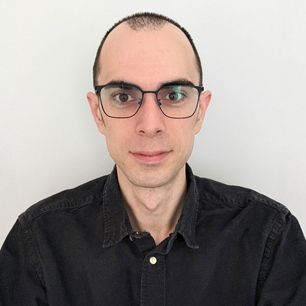
Milan Pešić
Senior Member of the Technical Staff and Director of Technology Development, Applied Materials Inc.
Bio:
Milan D. Pešić received a Ph.D. from the Technical University of Dresden, Germany, and is currently a Senior Member of the Technical Staff and Director of Technology development at Applied Materials Inc. He is leading a device and reliability team and overseeing device and cell physics and research activities in the field of advanced logic, (emerging) (non)volatile memories and devices. Previously, he was with MDLSoft Inc., Santa Clara, USA, Ferroelectric Memory Company, Dresden, and NaMLab, Dresden. Up to now, he has given 12 invited talks and (co)authored over 70 technical papers, four book chapters, and filed over 30 patents.
Abstract :
Only understanding of the materials and underlying physical mechanism can help us engineer novel superior devices of the future. Lead by this principle, we will look at ferroelectric (the most efficient memory material) and oxide-semiconductor materials and devices. We'll review what challenges they need to overcome to be integrated into logic and memory architectures. We will look in detail at the material phases, defects, vacancies, material changes, and underlying physical mechanisms governing mobility, variability, reliability, and others figures of merit of the devices they are integrated to.
Abstract:
Only understanding of the materials and underlying physical mechanism can help us engineer novel superior devices of the future. Lead by this principle, we will look at ferroelectric (the most efficient memory material) and oxide-semiconductor materials and devices. We'll review what challenges they need to overcome to be integrated into logic and memory architectures. We will look in detail at the material phases, defects, vacancies, material changes, and underlying physical mechanisms governing mobility, variability, reliability, and others figures of merit of the devices they are integrated to.
Toshiro Hiramoto
Professor, The University of Tokyo
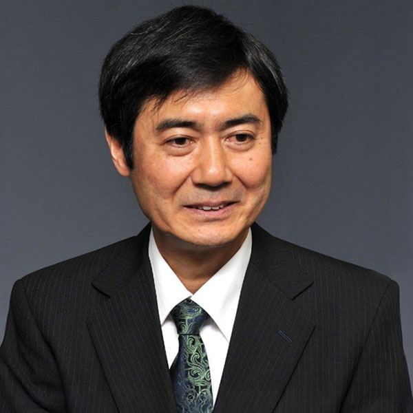
Toshiro Hiramoto
Professor, The University of Tokyo
Bio :
Toshiro Hiramoto received the Ph.D. degree in electronic engineering from the University of Tokyo in 1989. He joined Institute of Industrial Science, the University of Tokyo in 1994, where he has been a Professor since 2002. His research interests are various scaled silicon devices including FDSOI and nanowire FET as well as their statistical characteristics.
Abstract :
We have fabricated nanosheet oxide semiconductor FETs with sub-100nm gate length and the statistical variability data were compared with those of bulk planar Si MOSFET.
Milind Weling
Head of Lab-to-Fab-to-Product Realization, Merck
Milind Weling
Head of Lab-to-Fab-to-Product Realization, Merck
Bio :
Milind Weling is the Head of Lab-to-Fab-to-Product Realization and co-founder of the Neuro-inspired Computing Incubator of the Electronics business of Merck KGaA, Darmstadt, Germany, and for EMD Electronics in the U.S. and Canada. Previously he was Senior Vice President for Intermolecular, Inc. where he led Customer Programs and Operations where he drove the discovery and optimization of new materials, integrated module solutions, and leading-edge devices. Milind is a senior engineering and management professional with extensive experience in advanced memory and logic technology development, DFM and design-process interactions, new product introduction, and foundry management. His previously held senior engineering and management roles include DFM products engineering at Cadence Design Systems and high-performance CMOS technology development at Sun Microsystems, Philips Semiconductors, and VLSI Technology. Milind holds a B. Tech and MS degrees in Electrical Engineering from the Indian Institute of Technology, Bombay, and the University of Hawaii, respectively. He holds 50+ patents and has co-authored over 70 technical papers, primarily focused on semiconductor process technology, integration and semiconductor device reliability.
Abstract :
The advent of artificial intelligence (AI) has had a disruptive impact on the state of the art of technology at all levels of abstraction. AI’s explosive growth demands significantly revolutionary and enabling improvements of >100X for memory density + bandwidth, latency + performance, and energy consumption + overall environmental sustainability. With device innovation at its core, present day technology development focuses on emerging methodologies that require co-optimization of all orders of abstraction such as system, design, devices, technology and even materials aka SDDTMCO. This talk will highlight the opportunities and challenges the industry faces in transitioning from established to novel process architectures that require new materials for successful deployment. Our ability as materials suppliers to offer integrated additive process modules that meet customers’ aggressive performance and reliability target key performance indices (KPIs) will be crucial to accelerating semiconductor technology development. Moreover, technological progress can be further accelerated by embracing digital transformation to explore our exploration space and enable innovation.
Hitoshi Wakabayashi
Professor, Tokyo Institute of Technology
Hitoshi Wakabayashi
Professor, Tokyo Institute of Technology
Bio :
He is now the Leader and Professor of Integrated Green-niX+ Research Unit, Institute of Innovative Research, Tokyo Institute of Technology (Tokyo Tech). After NEC, MIT and Sony, he has joined Tokyo Tech since 2013, and had served as Director of Research Institute for the Earth Inclusive Sensing and the Member of the Education and Research Council. He also serves as the Research Supervisor of JST-PRESTO, the Deputy Leader of Device Tech. Div., Leading-edge Semiconductor Technology Center, Associate Member of Science Council of Japan, and the Chair of Conference on Ion-Implantation Tech. 2024. He had also engaged in the Directors of JSAP, JIEP, Japan MOT Society, Symp. on VLSI Tech., EDTM, IWJT and IEEE/EDS/VLSI Tech. & Circuits Committee.
Abstract :
2D transition-metal di-chalcogenide (TMDC) devices formed by physical-vapor deposition (PVD) method will be discussed for chiplet systems. Especially, MoS2, WS2 and ZrS2 FETs will be disclosed for future 3D-stacked FET and CFET. Furthremore, WS2 thermoelectric generators will be also shown for chiplet systems.
Simone Bertolazzi
Principal Analyst, Memory, YOLE GROUP
Simone Bertolazzi
Principal Analyst, Memory, YOLE GROUP
Bio :
Simone Bertolazzi, PhD, is Principal Analyst (Memory) at Yole Group. As member of the Yole Group’s Memory team, he contributes on a day-to-day basis to the analysis of markets and technologies, their related materials, device architectures and fabrication processes. Previously, Simone carried out experimental research in the field of nanoscience and nanotechnology, focusing on emerging semiconducting materials and their opto-electronic device applications. He (co-) authored more than 20 papers in high-impact scientific journals and was awarded the Marie Curie Intra-European Fellowship. Simone obtained a PhD in physics in 2015 from École Polytechnique Fédérale de Lausanne (Switzerland) and a double M. A. Sc. degree from Polytechnique de Montréal (Canada) and Politecnico di Milano (Italy).
Abstract :
In this presentation, I will provide an overview of emerging non-volatile memory (NVM) markets and technologies, discussing their technical maturity and their recent progress towards mass adoption in stand-alone and embedded applications. After reviewing the different NVM solutions currently available at leading semiconductor foundries/IDMs – among which MRAM, ReRAM, and PCM – I will discuss the challenges and opportunities for their adoption as embedded NVM in microcontrollers and edge-AI devices.
RF & Telecommunications
Eric Mercier
Telecom Line Director, CEA-Leti
Eric Mercier
Telecom Line Director, CEA-Leti
Eric Mercier is Telecom Line Director at CEA-Leti as well as Deputy Head of the Wireless Unit. He is active in industrial partnership developments towards technology transfer and also in managing internal CEA-Leti program, amongst which the FAMES WP10 dedicated to demonstrators. Graduated from ENSEEIHToulouse, France, in 1991, and with a 1st experience in the Optical Test Equipment at Wavetek (1992 – 1998, now VIAVI), his main focuses of interest have covered activities from Low-Power IoT transceiver solutions as Marketing & Application Manager for Atmel (1999 – 2006, now Microchip), and later as Project Manager & Laboratory Head Manager at CEA-Leti from 2006. As a promoter of CEA-Leti RF/mmW research activities, he is committed to market & societal needs for next Telecom generation towards new technologies development, understanding how forthcoming scientific developments can be valued to that end.
Swan Gerome
RF & Telecommunications Industrial Partnership Manager, CEA-Leti
Swan Gerome
RF & Telecommunications Industrial Partnership Manager, CEA-Leti
Bio:
Swan GEROME is Technology Partnership Manager within the Systems Department, with a focus on RF and Telecommunications at CEA-Leti.
He holds a degree in Marketing and Sales Management from Grenoble IAE and has over 15 years of experience in the semiconductor industry across materials, design, and research companies.
From 2008 to 2014, he served as Sales Manager at Dolphin Integration, developing business for ASIC design, analog silicon IP, and libraries for foundries, fabless companies, design houses, and OEMs. He also managed a team of sales coordinators in Asia (Japan, South Korea, and Taiwan) as well as in Europe.
He joined CEA-Leti in 2015 as Industrial Partnership Manager for the Systems Department, covering sensor integration, energy management, embedded data processing, and RF telecommunications (antenna design and integration, protocols development, and RFIC design). In this role, he developed partnerships with national and international companies, ranging from startups to Big Tech.
Between 2022 and 2023, he was Product Marketing Manager for the Connect-SOI Business Unit at Soitec, where he developed the roadmap for engineered silicon substrates for RF applications and launched new products to address market requirements.
Perrine Batude
MOS & 3D Sequential Integration Expert, CEA-Leti
Perrine Batude
MOS & 3D Sequential Integration Expert, CEA-Leti
Bio :
Perrine BATUDE obtained her Ph.D. degree from the Institut National Polytechnique de Grenoble, France in 2009 during which she began the early development of 3D Sequential Integration (3DSI) in CEA-Leti. Since then, she participates to the development of this technology for various applications fields including computing, imagers, and RF. She is the author and coauthor of more than 130 publications in major conferences and journals and of more than 20 patents. Her field of expertise covers especially semiconductor devices, especially FD-SOI transistors, low temperature processes with a specific focus on low temperature junction processes, direct bonding for channel transfer.
Abstract :
Jean-Baptiste David
RF-mmW R&D Engineer, CEA-Leti
Jean-Baptiste David
RF-mmW R&D Engineer, CEA-Leti
Bio:
Jean-Baptiste David was born in 1973 and received his master of research in 1997. After various experiences in wide companies and a startup, he joined CEA Leti in 2002. His field of compentences is focused on RF-mmW IC design. Previously involved in BAW filters and duplexers, component modeling, electromagnetic simulation, 5G front-end modules, and control/readout IC for quantum computing, he is more recently involved in the design of frequency synthesis architectures on RFSOI and FDSOI technologies for 10GHz to 100GHz applications.
Yvan Morandini
Senior Strategic Marketing Manager, Soitec
Yvan Morandini
Senior Strategic Marketing Manager, Soitec
Bio:
Dr Yvan Morandini received the Degree in engineering from Grenoble Alpes University, France in electronics
and radiofrequencies in 2005 and the PhD degree from Lille University in 2008. After 3 years in
STMicroelectronics he then moved to IBM , Dolphin Integration and then to SOITEC. He is currently Senior Strategic Marketing Manager at SOITEC. He has 20 years of experience in
semiconductor industry including characterization, modeling and design. He has authored/co-authored over
15 papers in international, peer-reviewed journals and conferences, and is Member of Institute of Electrical
and Electronics Engineers (IEEE).
Abstract:
Wireless technologies are constantly evolving to meet the demands of new and emerging applications. The introduction of 5G and the forthcoming 6G wireless systems present significant challenges for the design and implementation of new RF front-end components. To keep pace with this evolution, it's crucial for semiconductor technologies to achieve the RF performance needed for the next-generation RF Front Ends (RFFE). In this presentation, we will discuss the RF technology roadmap, emphasizing engineered substrates that are key to designing the next generation of RFFE.
Kazuaki Deguchi
Senior Manager RF Device Division, Murata
Kazuaki Deguchi
Senior Manager RF Device Division, Murata
Bio :
Kazuaki Deguchi received the B.S. and M.S. degrees in electronics, information systems and energy engineering from Osaka University, Suita, Japan, in 2000 and 2002, respectively. From 2002 to 2014, he joined Renesas Electronics Corporation, Hyogo, Japan and engaged in research and development of analog and mixed-signal circuits. From 2012 to 213, he joined IMEC Leuven, Belgium as an expatriate to research high-precision ADC. From 2014, he has been working with Murata Manufacturing Co, Ltd., Kyoto, Japan. He initially engaged in Wi-Fi module design and since 2018 he has been working for RF device development. His recent research interests include the high-linearity and high-efficiency power amplifier design for RF front-end.
Abstract :
In the realm of RF Front-End products, there has been a historical emphasis on high data rates. However, real-world products have demonstrated a growing need for tailored solutions that align with specific use cases. This presentation will shed light on this paradigm shift and explore how RF Front-End Modules are evolving to meet application-specific requirements. We will delve into the world of RF Front-End Modules with a specific focus on three key aspects: economical, low power consumption, and user-friendliness RF Front-End Module solutions.
David Moussaud
R&D Engineer, CEA-Leti
David Moussaud
R&D Engineer, CEA-Leti
Bio :
David MOUSSAUD graduated from the Ecole Supérieur d'Électronique de l'Ouest (ESEO) in Angers in 2004, with a specialisation in embedded systems.
He worked as an embedded Linux engineer, first in Italy at Thales Communication, then as a consultant, in France in 2006 at Sagem Communication (Livebox products) and Nagra Kudelski (for access control of DVB decoders).
In 2008, he joined the CMMI 3 design office in Nantes, working mainly on automotive projects. He then joined a large Autosar team involved in the development of the basic softwares and the associated modelling tools. He focused mainly on the RTOS module and the integration of communication stacks.
Since 2014, he has been an R&D engineer at CEA-Leti in the wireless technologies department, in the signals, protocols and radio platforms laboratory. As a software developer, system architect or project manager, he has been involved in several projects aimed at developing wireless protocols for industrial IoT.
Abstract :
To remain competitive or to win new markets, companies need to upgrade their products, for example to simplify installation and operation, improve robustness, and/or add new functions such as remote software updates or monitoring. The use of wireless technologies is often one of the solutions needed to meet these challenges. And to make these products communicate in their environment, with the associated constraints, a communication protocol is needed. Depending on the constraints of the application and/or the operating environment, it is not always possible to identify an off-the-shelf solution or a standardized protocol that can meet the performance indicators imposed by the application. In this presentation, illustrated by several case studies, we will explain how we meet this need, and how we develop and transfer communications stacks for industrial IoT at high TRL levels.
Nicola di Pietro
Subsidized Project Specialist, HPE
Nicola di Pietro
Subsidized Project Specialist, HPE
Bio:
Nicola di Pietro has worked at the Athonet Research & Innovation department of HPE, Italy, since 2021. He has B.S., M.S., and Ph.D. degrees in mathematics, received respectively from the Univ. of Padova, Italy, in 2008, jointly from the Univ. of Padova, Italy, and the Univ. of Bordeaux, France, in 2010, and from the Univ. of Bordeaux, France, in 2014. He was a Research Engineer with Mitsubishi Electric in Rennes, France, between 2010 and 2013. From 2014 to 2016, he was an Associate Post-Doctoral Fellow at Texas A&M University at Qatar, and from 2017 to 2021 he was a Research Engineer with CEA LETI in Grenoble, France. His research focuses on 5G-and-beyond networks, edge cloud computing, and coding theory.
Abstract:
Private 5G networks meet the telecommunication service requirements of heterogeneous vertical sectors, proposing mobile networks as controllable and tuneable infrastructural assets for industrial, governmental, and commercial entities. Based on HPE's on-field experience, this presentation discusses private 5G use cases, edge-to-cloud network deployments, and technological enablers. It highlights the versatility of private 5G architectures and the increased automation, robustness, security, and control capabilities compared to other network technologies and previous mobile generations.
Laurent Dizambourg
Innovation Project Leader, Stellantis
Laurent Dizambourg
Innovation Project Leader, Stellantis
Bio:
Electronics Telecommunication and Hyperfrequencies, I began my carreer in 1998 in the development of RF communication modules for mobile networks. In 2002, I chose to move to automotive industry. During this last 22 years, I had the opportunity to lead several projects in development and in innovation the domain of Infotainment and Connectivity for PSA and then Stellantis.
Abstract:
As the off board communication system becomes more and more complex, with additional possible telecommunication chanels like Satellite connectivity, involving new frequency bands, the automotive industry shall keep competitiveness and efficiency in the design of their embedded systems. In Stellantis, the embedded architecture has been designed to allow this flexibility for current and future evolution of the connectivity needs.
Alexandre Giry
RFIC/PA Design Team Leader, CEA-Leti
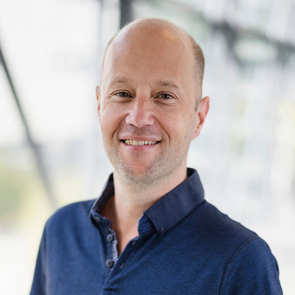
Jean-Philippe Fournier
CEO, Spectronite
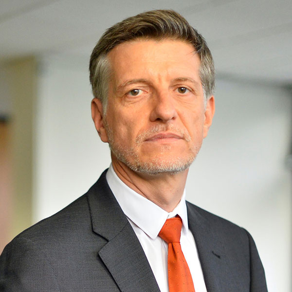
Jean-Philippe Fournier
CEO, Spectronite
Bio :
Jean-Philippe is the CEO and Founder of SPECTRONITE, a startup company introducing a new generation of transmission technology for the backbone of mobile networks.
The company introduces a software-powered radio system that allows for super-high-capacity transmission while enabling spectral control and network virtualisation.
Jean-Philippe has 25 years experience in the telecom market and has held the position of Director of Marketing, in charge of mobile operators at Texas Instruments and Head of Multimedia R&D group at Bouygues Telecom, French mobile operator.
Jean-Philippe holds 8 patents and received a degree in Digital Signal Processing from the University of Valenciennes and in a Applied Physics from the University of Le Havre, France.
Abstract :
Traditional transmission techniques have long been able to deliver sufficient capacity for mobile operators to roll-out mobile services.
With the advent of 5G, increased pressure for sustainable networks and the increasing need to share spectrum among multiple applications (mobile RAN, backhaul, WiFi), new techniques are required for the delivery of high-speed services.
This talk details how SPECTRONITE's software powered-architectures helps operator to take up the challenge.
Yu-Ju Chuang
Senior Technical Manager, ITRI
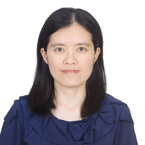
Yu-Ju Chuang
Senior Technical Manager, ITRI
Bio :
Yu-Ju Chuang received her Ph.D. degree in electrical engineering from University of Illinois at Urbana-Champaign in 2007. From 2007 to 2009, she worked in Skyworks and engaged in the design of PA and FEM for cellular handset. Then she joined Ralink Technology, which was later merged with Mediatek, focusing on the development of Bluetooth and WiFi transmitter and power amplifier. Since 2013, she has been working with Industrial Technology Research Institute (ITRI) and her research interest involves RF and mmWave transceiver IC for 5G and satellite communications.
Abstract :
Nowadays, LEO satellite communication is gaining more and more interest. For the communication payload, it is crucial to keep the power consumption of the transceiver low due to limited power supply by the solar panel. The rough and radiation-rich environment in space also presents significant challenges to the implementation of the RF ICs. In this presentation, we will discuss the requirement and development status of our RF chipsets for Taiwan's B5G LEO communication payload. Some related work in RF circuit and module design developed in ITRI will also be presented.

