Speakers
Sébastien Dauvé
Chief Executive Officer, CEA-Leti
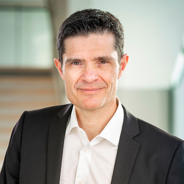
Sébastien Dauvé
Chief Executive Officer, CEA-Leti
Bio:
Sébastien Dauvé was named CEO of CEA-Leti effective on July 1, 2021, after more than twenty years of experience in microelectronics technologies and their applications, including clean mobility, medicine of the future, cybersecurity, and power electronics.
Sébastien Dauvé started his career at the French Armament Electronics Center, where he worked on developing synthetic-aperture radar. In 2003, he joined CEA-Leti as an industrial transfer manager and supervised several joint research laboratories, in particular with the multinational Michelin.
In 2007, Sébastien Dauvé became a laboratory manager, then head of an R&D department in the area of sensors applied to the Internet of things and electric mobility. During this time, he supported the dissemination of new technologies in industry, including the automotive industry (Renault), aeronautics, national defense (SAFRAN), and microchips with the industry leader Intel. He played an active role in the creation of start-ups in application fields ranging from health to infrastructure security, leading to dozens of new jobs. In 2016, he became Director of the CEA-Leti Systems Division.
From sensors to wireless communication, Sébastien Dauvé has played an active role in the digital transformation, focused on coupling energy frugality and performance. He has made cross-disciplinary approaches central to innovation by harnessing the expertise of talented teams with diverse backgrounds. Their goal is to provide technological tools for meeting the major societal challenges of the future.
Sébastien Dauvé is a graduate of the French Ecole Polytechnique and the National Higher French Institute of Aeronautics and Space (ISAE-SUPAERO).
Abstract:
At CEA-Leti, innovation is not just our aspiration—it’s part of our DNA. For decades, we have been developing technologies that have enabled the semiconductor industry to new heights, now embedded in everyday applications such as smartphones, automobiles, and healthcare.
Today, technology goes beyond products—it has become a matter of geopolitics and sustainable development. Artificial Intelligence, in particular, is reshaping the landscape and opening up a new field of possibilities.
With the strong support of France and Europe, CEA-Leti is more determined than ever to continue its role as a pioneer, serving both industry and society. We are committed to advancing next-generation semiconductor technologies, co-developing with our partners safer, more energy-efficient, and sustainable solutions to meet today’s pressing challenges.
This keynote will explore how CEA-Leti is shaping a more competitive, ethical, and sustainable digital future—turning visionary ideas into impactful realities.
Dr. Ahmad Bahai
SVP & CTO, Texas Instruments
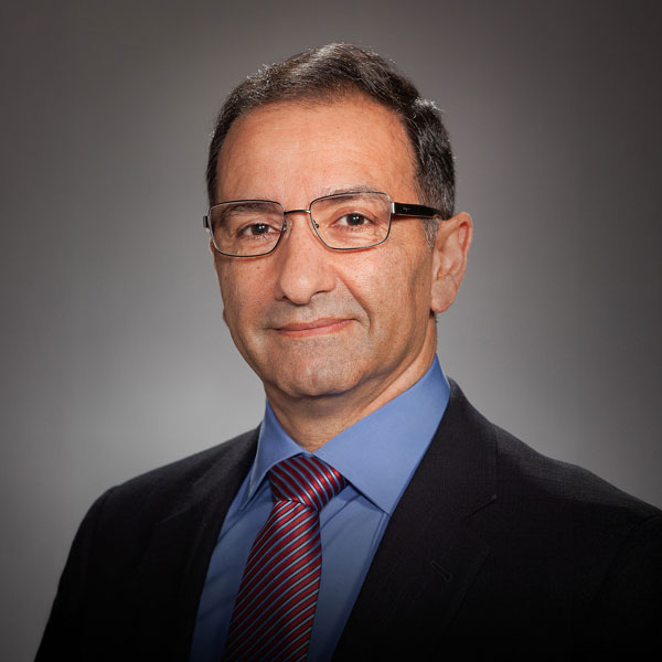
Dr. Ahmad Bahai
SVP & CTO, Texas Instruments
Bio:
Dr. Ahmad Bahai is the Senior Vice President and Chief Technology Officer (CTO) at Texas Instruments, where he leads groundbreaking innovation, corporate research, and Kilby Labs.
He also serves as a Professor of the Practice at the Massachusetts Institute of Technology (MIT), is an IEEE Fellow, and is a member of the Industrial Advisory Committee for the CHIPS Act. Previously, Dr. Bahai contributed to the President’s Council of Advisors on Science and Technology’s semiconductor working group. From 2017 to 2022, he was an Adjunct Professor at Stanford University and, from 2001 to 2010, a Professor in Residence at UC Berkeley.
Dr. Bahai’s technology leadership experience includes roles as Director of Research Labs and CTO at National Semiconductor, Technical Manager of a research group at Bell Laboratories, and Founder of Algorex, a communications and acoustic IC and systems company acquired by National Semiconductor.
He has authored over 80 publications in IEEE/IEE journals and holds more than 40 patents related to systems and circuits. Dr. Bahai earned a Master of Science in Electrical Engineering from Imperial College, University of London, and a Ph.D. in Electrical Engineering from the University of California, Berkeley.
Abstract:
Advancements in semiconductor technology, along with improvements in analog and digital signal processing, connectivity, battery technology, and security, have accelerated the deployment of intelligent sensing and actuation across diverse applications. However, nature often offers more efficient edge computing solutions by leveraging hierarchical signal processing to enhance performance and minimize energy consumption in intelligent sensory systems.
In this talk, we explore cutting-edge examples of low-power machine learning at the extreme edge, including bio-inspired sensor fusion. We will examine how innovations in devices, circuits, and machine learning systems are converging to drive the next generation of intelligent, energy-efficient sensing and actuation technologies.
Kaïs Mnif
CEO, Trixell
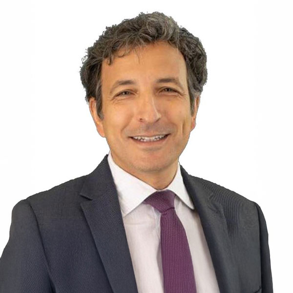
Kaïs Mnif
CEO, Trixell
Bio:
Kaïs Serves as CEO to Trixell, a joint venture between Thales, Siemens, and Philips specialized in X-ray flat panel detectors. He's also Head of the Radiology business at Thales.
Kaïs joined Thales in 2014 in Singapore as Business Development Director covering Asia. He then led the air traffic navigation aids Business of Thales, based in Milan.
Before joining Thales, he spent 18 years in the Automotive then the Railway industry where he held several management positions around the world.
Kais holds an engineering degree in automation and electronics from INSA Toulouse, a Master degree in enterprise administration from IAE Toulouse, and an MBA from INSEAD.
He's occasionally a guest lecturer in decision sciences, and multicultural leadership.
Abstract:
A bit like the concept of 'terroir' in wine making defines the unique combination of environmental factors and human practices in a specific location, industrial clusters are sometimes born from similar unique combinations.
Trixell was born from such favorable combinations of environmental factors : proximity with CEA and top universities, facilitated access to a large local talent pool, and a rich regional supply chain, to mention a few.
My presentation will quickly describe how about 30 years ago the flat panel detector was invented here, and why the next innovations in X-Ray imaging will continue to be invented here and what we're doing about it together with the CEA.
Hervé Bouaziz
President, Lynred
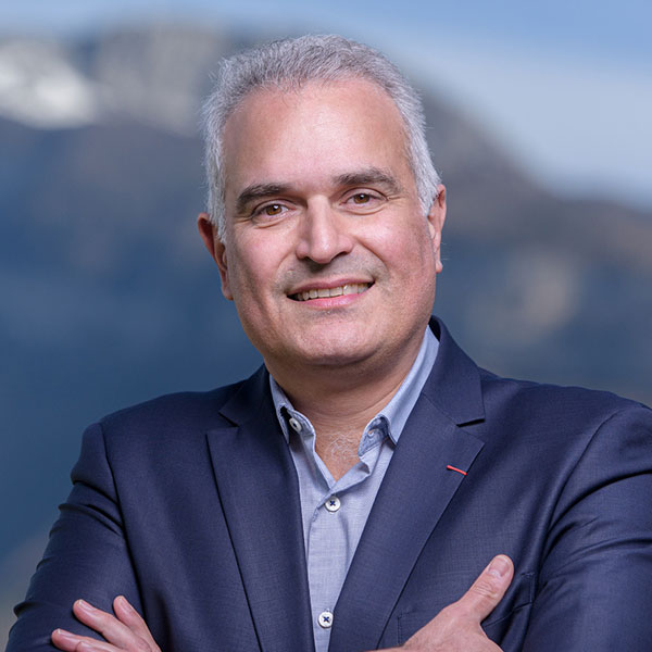
Hervé Bouaziz
President, Lynred
Bio:
Hervé Bouaziz was appointed executive President of LYNRED, a world leader in Infrared detectors, in December 2023. Prior to that he held various positions of responsibility within SAFRAN Group, as Director of Strategy and M&A within Safran Electronics and Defense, and as Director of Military Engines Programs within Safran Aircraft Engines. He also worked 20 years in Aerospace at DGA, the Defense Armament Procurement Agency of the French Ministry of Defense, on military aircraft Programs and as an Armament Attaché in Washington DC. Hervé is a graduate of Ecole Polytechnique, SupAéro, and the Industrial Colllege of the Armed Forces (USA). He also earned his wings as a military pilot in the Armée de l'Air et de l'Espace.
Abstract:
Infrared sensing and imaging is a fast expanding market due to its inherent unique characeritics
Trend is clearly toward high resolution, miniaturization, low power consumption and agile image correction with AI
Anticipation of high demand in mobility, industrial control, environment, Robotics, with applications involving the use of AI
Generalization of usage will draw a strong requirement for better competitivity, and high volume production capacity
LYNRED is gearing up to meet this challenge with its partners and its brand new CAMPUS manufacturing capability
Deirdre Hanford
CEO, NATCAST

Deirdre Hanford
CEO, NATCAST
Bio:
In January 2024, Deirdre Hanford was appointed Chief Executive Officer of Natcast, the operator of the National Semiconductor Technology Center (NSTC). Established by the U.S. CHIPS and Science Act, the NSTC is a public-private consortium driving U.S.-led semiconductor innovation and economic and national security.
Prior to Natcast, Hanford served as an executive at Synopsys in a career spanning over thirty-six years. She has served on many industry advisory boards, including being a leader in the Department of Commerce Industrial
Advisory Committee formed through the CHIPS Act.
Among her industry accolades, Hanford was selected to receive the 2025 IEEE Frederik Philips Award “for visionary leadership in electronic design automation
for secure and energy-efficient microelectronics” in July 2024.
Hanford earned a B.S. Engineering (electrical engineering) from Brown University and an M.S.E.E. from University of California, Berkeley.
Abstract:
Semiconductor R&D continues to present enormous opportunity in developing the technologies of tomorrow. Deirdre Hanford will discuss the need for cross-industry collaboration and innovation at all levels of the semiconductor stack, including the role of the recently established U.S. National Semiconductor Technology Center (NSTC) in convening stakeholders from across the ecosystem; fostering the development of a skilled workforce; and its exploration of semiconductor research in the AI era.
Barbara De Salvo
Director of Research, Meta Reality Labs
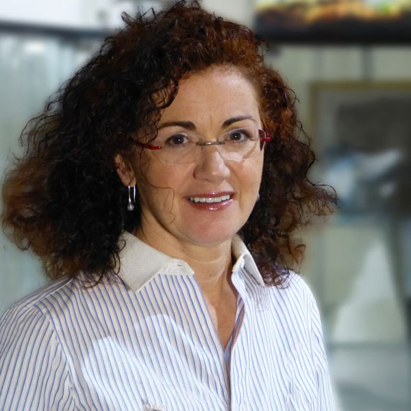
Barbara De Salvo
Director of Research, Meta Reality Labs
Bio:
Barbara De Salvo is Director of Research at Meta Reality Labs Research, responsible for new AI sensing technologies, novel low-power systems and ML architectures for Smart glasses and future Augmented Reality glasses. Before joining Meta in 2019, she was Chief Scientist and Deputy Director of CEA-LETI, driving the path-finding strategy. In 2013-2015, she was visiting scholar in IBM-Albany-NY in the frame of the sub-10nm CMOS International Technology Alliance, where several of her research works have led to product technologies for novel logic ICs (as Silicon-On-Insulator, Finfet and stacked nanowire technology platforms). In CEA-LETI, she founded and led the advanced memory technology division (2008-2013), where she promoted the introduction of disruptive memory technologies, such as phase-change memories, resistive oxide-based and conductive-bridge memories. She pioneered neuromorphic hardware solutions based on emerging technologies for ultra-low-power cognitive systems. She has authored more than 400 referred articles, ten book chapters, a monography on Silicon Non-Volatile Memories edited by Wiley and Sons and several patents. She served as General Chair of IEEE IEDM 2022, as well as chair of the IEEE Corporation Award Committee from 2022 to 2024, in the Fellow Evaluation Committee, IEEE nanotechnology in 2024-25. She is a fellow of IEEE.
Abstract:
All-day wearable, fashionable smart and AR glasses will transform the ways in which we live and work. In this presentation we will look at an example of wearable system architecture, and how AI sensor could play a critical role for future Contextual AI wearable device.
Jean-René Lèquepeys
Deputy Director and Chief Technology Officer, CEA-Leti
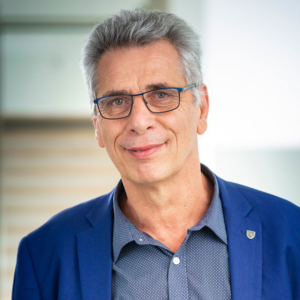
Jean-René Lèquepeys
Deputy Director and Chief Technology Officer, CEA-Leti
Bio:
Jean-René Lèquepeys received an engineering degree in 1983 from CentraleSupélec, a top French graduate engineering school at Paris-Saclay University, France. He taught physics during 2 years in Ouarzazate, Morocco.
He joined CEA, a French Research and Technology Office focusing on applied research, in Paris Saclay in 1985. He first worked at the laboratory of the Central Security Office, on the evaluation of means of detection and intrusion. Two years later, he was promoted head of this laboratory.
In 1993, he moved to Grenoble, France, and joined the System Division of CEA-Leti. He worked on different projects in the field of image processing and telecommunication technologies. In particular, he was responsible for the "Telecom, Communicating Objects and Smart Card" programs from 1999 to 2004.
In 2005, he took the responsibility of the Circuits Design Division at CEA-Leti (200 people). He launched new research activities at CEA such as a new laboratory in Aix-en-Provence, France, on the development of secured chips. In 2000, Jean-René Lèquepeys received the prestigious award from the french Société de l'Electricité, de l'Electronique et des technologies de l'information et de la communication (SEE) "Grand Prix de l'électronique Général Ferrié" for his work in the telecommunications field (he holds 15 patents).
In 2010, he launched a new division at CEA focusing on Electronic Architectures, Integrated Circuit Design and Embedded Software. He established the structure on two sites (Paris and Grenoble) and led the division twice in his career.
He rapidly got involved in the creation of the Silicon Components Division at CEA-Leti, and took the lead of it in 2011 managing 350 people. Division encompasses micro and nanoelectronics (SOI, nanodots, quantum, memories, 3D technologies, substrates), Micro Systems (sensor, actuator, radiofrequency components) and Power Components. He established the French Nano2022 Program for research funding in microelectronics.
In 2019, he was appointed Chief Technology Officer of CEA-Leti, overseeing Science, relations with the European Commission, Industrial Partnership and Strategic Program Management in the scope of the institute (2,000 people, ~€350m budget). He took the responsibility of the Microelectronic Program at CEA level, spearheading technological and upstream research in the field of semiconductor technologies. For the past 2 years, he has been strongly involved in the CEA-Leti Next Gen FD-SOI project in the frame of France2030 and has played a key role in European chips Act pilot line promoting FD-SOI and Gate All Around technologies.
Having dedicated his career to applied research, he is regularly invited as a keynote speaker in international semiconductor conferences.
Jean-René is also Vice President of ACSIEL, a professional trade union gathering industrial companies in the French electronic value chain, member of the Board of EPOSS, the European Technology Platform on Smart Systems Integration, a member of the Board of AENEAS, the Association for Europoean NanoElectronics Activities, and an expert consultant for the European Commission and French Research Agency
Abstract:
Chips are ubiquitous in our current digital world, and semiconductor applications cover a wide range of societal needs. From smart sensors and the Industrial Internet of Things to digital cities and factories, personalized medicine, precision agriculture, vehicle electrification and automation, the cloud, high-performance computing, and the defense sector. How can we pursue digitalization and build a sustainable world while taking into account a limited energy budget and planetary boundaries?
This keynote will explore how we manage exponential data growth sustainably. How can we pursue digitalization and build a sustainable world while taking into account a limited energy budget and planetary boundaries? Highlighting recent breakthroughs from CEA-Leti, we showcase tangible progress towards a greener, more sustainable semiconductor future. A structuring initiative with a 1000x energy efficiency gain will be proposed leveraging on advanced CMOS technologies, disruptive chips architectures, novel computing paradigms, and optimized algorithms, we demonstrate concrete pathways towards dramatically reduced energy usage.
Herman Boom
Executive Vice President Business Line DUV, ASML
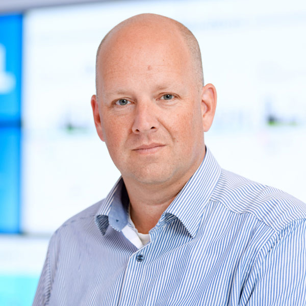
Herman Boom
Executive Vice President Business Line DUV, ASML
Bio:
Herman was appointed as Executive Vice President in September 2018, leading Development and Engineering. On April 1st 2022 he was appointed Head of Business Line DUV
He joined ASML as from February 1997. He held various positions from engineering, project management, product development and program management for EUV programs, Twinscan-, DUV-, and immersion programs.
Herman graduated from TU Eindhoven Applied Physics after finalizing a master projects on semi-conductor optics in cooperation with Semiconductor physics group of RWTH Aachen.
Abstract:
AI is everywhere, requiring more data ingestion and compute than ever, driving a breath of applications and semicon requirements – both in leading edge and mainstream.
Core challenges for the ecosystem are energy efficiency, affordability, and scalability of the periphery.
ASML aims to address these in our innovations & product roadmap, as well as by architecting More than Moore solutions.
On the other side of the spectrum, ASML is also deploying AI across the company & operation. Herman will share the landscape of ASML AI domains, as well as concrete examples and their progression over time.
Thibault Basquin
Member of the Executive Committee & Co-Head of Buyout, ARDIAN
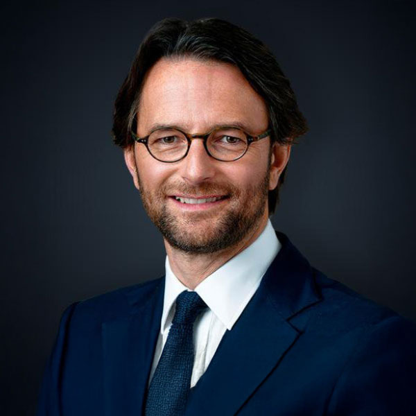
Thibault Basquin
Member of the Executive Committee & Co-Head of Buyout, ARDIAN
Bio:
Thibault is Member of the Executive Committee of Ardian and Co-Head of Ardian Buyout. He also oversees the recently launched Ardian Semiconductor platform initiative.
He joined Ardian in 2001 and has led many successful transactions. In 2018, he moved to New York to launch the US Buyout group. In 2010, Thibault contributed strongly to the launch of the Ardian Foundation. He began his career in 2000 at Arthur Andersen as an auditor.
Thibault graduated from ESCP Europe in Paris with a master's degree in Finance.
Since 2020, he is a also a member of the Board of Trustees of L'Alliance New York, as well as the ESCP Foundation Inclusion & Diversity Committee in Paris.
His family is based in New York since 2018 and he splits his time between New York and Paris.
Abstract:
The global semiconductor market is projected to reach $1 trillion by 2030, driven by digitalization, AI, mobility electrification, and connectivity. Geopolitical tensions, particularly US-China decoupling and defence spending spree are creating opportunities for EU companies to gain market share and diversify their customer base. Europe, with its unique R&D capabilities and market-leading companies is poised to benefit from these trends if it succeeds in accessing the financing firepower required.
Michael Tchagaspanian
EVP Strategic Partnership, CEA-Leti
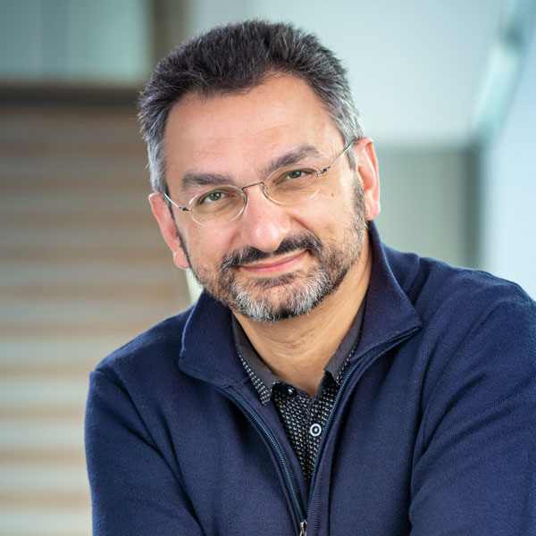
Michael Tchagaspanian
EVP Strategic Partnership, CEA-Leti
Emmanuel Le Taillandier de Gabory
General Manager, NEC Corporation
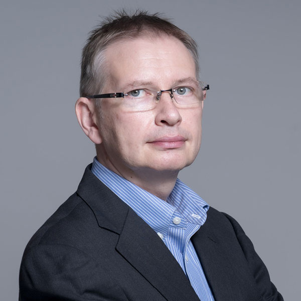
Emmanuel Le Taillandier de Gabory
General Manager, NEC Corporation
Bio:
Emmanuel Le Taillandier de Gabory was born in Libourne, France, in 1975. He received a MSc from the École Supérieure d’Optique, Orsay, France, in 1999 and an EMBA from Waseda University in 2018. From 2000 to 2007, he worked with Fujitsu Quantum Device Ltd., Yamanashi, Japan. In 2007, he joined NEC Corporation, Kanagawa, Japan, where he is currently the General Manager heading Advanced Network Research Laboratories. The research activities of his laboratories cover high capacity optical transport systems, digital signal processing for communication, quantum cryptography, space communication, beyond 5G mobile communication and applied sensing.
He has authored and coauthored more than 80 papers and 30 patent applications. He is a senior member of the IEICE (Japan) and he has been serving in technical committees of major conferences in the communication field.
Abstract:
In this talk, we will explore the transformative potential of AI technologies, including generative AI, for communication networks. We will discuss how these technologies can drive growth, enhance efficiency, improve performance, and transform communication infrastructure. Additionally, we will address the critical challenges posed by AI infrastructure requirements for communication technologies.
Erik Hadland
Director of Technology Policy, SIA
Erik Hadland
Director of Technology Policy, SIA
Bio:
Erik Hadland is the Director of Technology Policy at the Semiconductor Industry Association (SIA), where he is responsible for the association’s research, development, and technology activities as well as its education and workforce development efforts. In this role, he works with the White House, Federal agencies, and Congress to inform policymakers about the needs and functions of the diverse segments of the semiconductor industry.
Prior to SIA, Erik was a AAAS Science and Technology Policy Fellow at the U.S. Department of Energy, where he served as Advisor to the Director of the Office of Science—the Nation’s largest supporter of fundamental physical science research and stewarding office of 10 of the Department’s National Laboratories. In this capacity, Erik project managed briefings to the Congress on critical and emergent technologies, advised on matters of place-based innovation and technology transfer, and co-facilitated the Department’s Microelectronics Working Group. Prior to the DOE, Erik was a Senior Logic Technology Development Engineer at Intel, piloting first-of-a-kind annealing modules and processing conditions for Intel’s next generation logic products.
Erik earned his PhD in Solid State Chemistry from the University of Oregon, where he studied novel synthesis schemes for metastable 2D semiconductor compounds.
Jörg Doblaski
CTO, X-FAB group
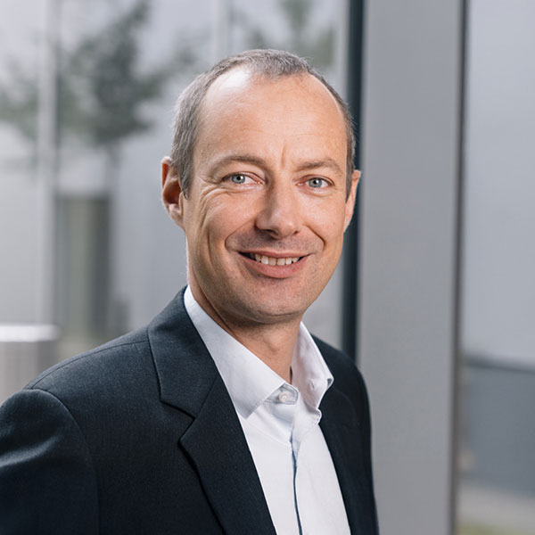
Jörg Doblaski
CTO, X-FAB group
Bio :
Jörg Doblaski joined X-FAB in 2004 and served in several different engineering- and R&D management positions before he was appointed as Chief Technology Officer in 2020. As the CTO, Jörg is responsible for the technology development within the X-FAB foundry group, including design- and prototyping support, and as well he is in charge of the group IT. He holds a diploma degree in Electrical Engineering and Information Technology from Technical University of Ilmenau, Germany.
Abstract :
Artificial Intelligence is being rapidly adopted in the industry. Like many other companies, X-FAB applies AI in operations and R&D to accelerate problem-solving, reduce waste, and increase yield. As a specialty foundry focused on More Than Moore technologies, X-FAB is also involved in enabling future AI solution. In the presentation, Joerg will provide insides into these aspects and share how X-FAB contributes to advance AI solutions, from lowest-power in-memory computing at the very edge to large-scale computing at the cloud.
Ashkan Seyedi
Director, Optical Interconnect Products, NVIDIA
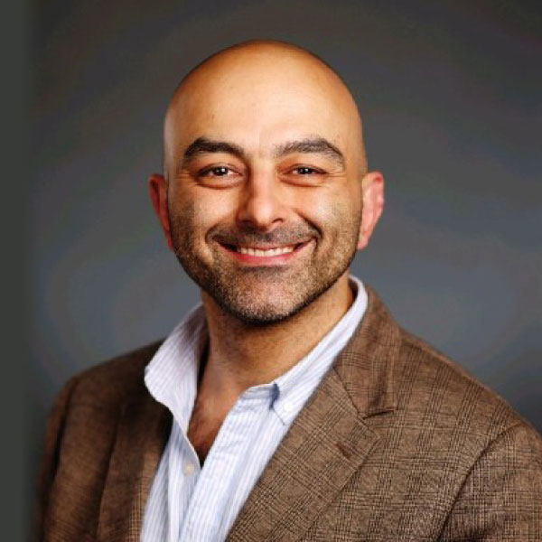
Ashkan Seyedi
Director, Optical Interconnect Products, NVIDIA
Bio:
As the Director of Silicon Photonics Products at NVIDIA, Ashkan Seyedi is at the vanguard of merging photonics with cutting-edge computing architectures, particularly in the spheres of generative AI and machine learning. Seyedi's expertise in silicon photonics is pivotal to the advancement of hardware technologies that underpin large language models and AI computations.
Since June 2023, he has spearheaded the integration of multidisciplinary teams to create interconnect solutions for next-generation GPU and CPU products. Prior to this, Seyedi served as a Silicon Photonics Product Architect at NVIDIA, where he played a crucial role in developing interconnect technologies over two years.
Before joining NVIDIA, Seyedi was a Senior Research Scientist at Hewlett Packard Labs, where he led a team in developing a commercial process design kit (PDK) for silicon photonics. His tenure there, spanning nearly seven years, included managing projects funded by various US Government agencies and collaborating with external companies on new products and software tools for electronic design automation.
Seyedi holds a Ph.D. from the University of Southern California, where he conducted groundbreaking research in nanowire photodetectors, solar cells, and LEDs, contributing significantly to the field of photonics. His early career also includes a stint as a Testing Intern at Intel Labs, where he worked on silicon modulators and integrated III-V lasers, achieving milestones in high-speed optical communications.
Abstract:
Yoshinami Takahashi
COO & Head of Global Solution Business Group, Fujitsu
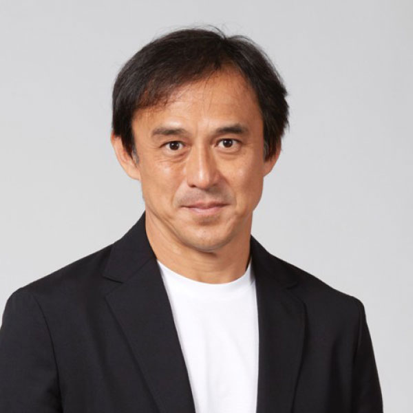
Yoshinami Takahashi
COO & Head of Global Solution Business Group, Fujitsu
Bio:
Yoshinami Takahashi joined Sony Corporation in 1987 and was involved in overseas business in the consumer division, including postings in North America and Europe, and served as an officer at overseas bases. He joined Microsoft Japan Corporation in 2014, leading the cloud market, partner collaboration, and DX support for enterprise customers. Since June 2021, he has been leading the Fujitsu Uvance business as Managing Executive Officer.
Abstract:
Pierre Barnabé
CEO, Soitec
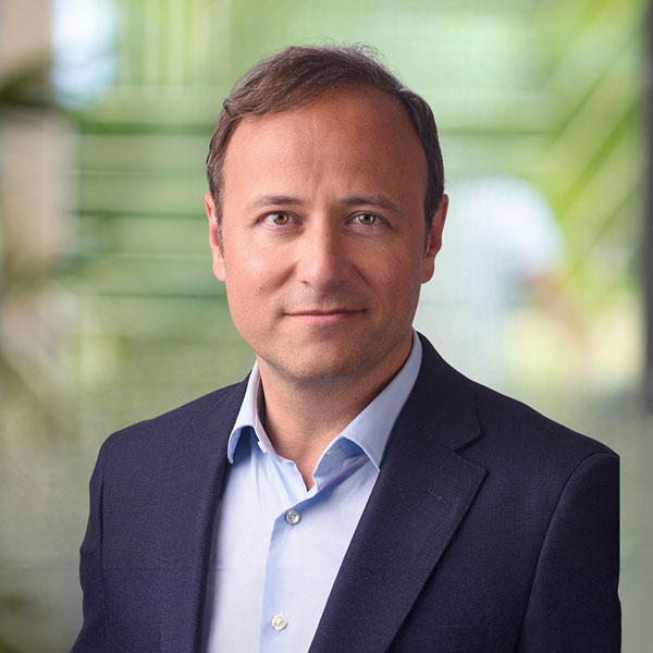
Pierre Barnabé
CEO, Soitec
Bio:
Pierre Barnabé was nominated as Soitec CEO in January 2022 and joined the company four months later.
He was previously Executive Vice-President in charge of Big Data & Cybersecurity at technology group Atos (2015-2021), where he also led the Public Sector & Defense division and manufacturing operations before serving as interim Group CEO in 2021.
Prior to its acquisition by Atos in 2014, Pierre Barnabé was Deputy CEO of Bull. He then served as Bull’s Chairman & CEO from 2015 to 2021, spearheading the company’s evolution into a global leader in cybersecurity services and supercomputing.
From 2011 to 2013, he was Managing Director of the Enterprise branch of SFR, the French telecoms operator, where he launched cloud computing and very high-speed broadband activities.
That followed a 13-year stint during which he held various positions at Alcatel and Alcatel-Lucent, first in sales and later as Chairman & Managing Director of Alcatel-Lucent France (formerly Alcatel CIT) and Group Deputy Managing Director for Human Resources and Transformation.
A graduate of the NEOMA Business School and Ecole Centrale in Paris, Pierre Barnabé began his career in 1994 in Silicon Valley, developing corporate venture capital and capital risk activities for Thales Group. He then moved to Thales headquarters in Paris, where he was in charge of strategy and acquisitions for the Communication and Command division.
A member of the board of the multinational market firm Ipsos, he also served as Chairman of the Board of ENSIMAG Grenoble, the prestigious Grande École specializing in computer science, applied mathematics and telecommunications (2016-2022) and on the board of France’s National Institute for Research in Digital Science and Technology (INRIA) from 2021 to 2022. Pierre Barnabé is a Knight of the French National Order of Merit.
Remi El-Ouazzane
President, Microcontrollers, Digital ICs and RF products Group, STMicroelectronics
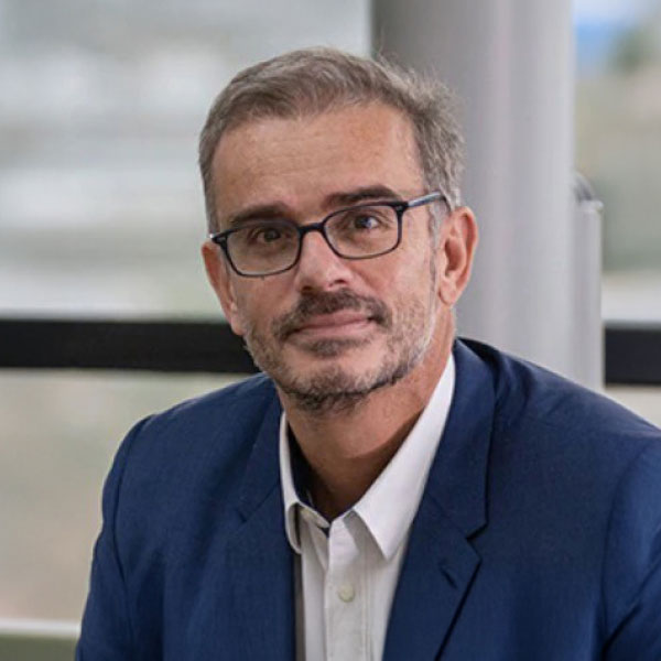
Remi El-Ouazzane
President, Microcontrollers, Digital ICs and RF products Group, STMicroelectronics
Bio :
Remi El-Ouazzane is STMicroelectronics’ President, Microcontrollers, Digital ICs and RF products Group and has held this position since February 2024. He is a
member of ST’s Executive Committee.
El-Ouazzane started his career at Texas Instruments in 1997. He rose through the ranks across the broadband, mobile, and embedded processing divisions to become Vice President and General Manager of the Open Multimedia Applications Platform (OMAP) in 2009. El-Ouazzane was appointed CEO of Movidius in 2013, responsible for driving its vision-processing technologies to advance the adoption of AI in the Internet of Things. With the acquisition of Movidius by Intel in 2016, he joined Intel’s
New Technology Group as Vice President and General Manager, and became Chief Operating Officer of Intel’s Artificial Intelligence Products Group in 2018. In 2020, ElOuazzane became Intel’s Datacenter Platform Group Chief Strategy Officer, driving
strategic initiatives in the data center and cloud markets.
In 2009, El-Ouazzane was honored with the French-American Foundation’s Young Leaders Award.
Remi El-Ouazzane was born in Neuilly-sur-Seine, France in 1973 and graduated from the Grenoble Institute of Technology (INPG) in 1996 and the Grenoble Institute of Political Studies in 1997. He graduated from the General Management Program
at Harvard Business School in 2004.
Abstract :
David Haynes
VP Strategic Marketing & Specialty Technologies Strategy, Lam Research Corporation
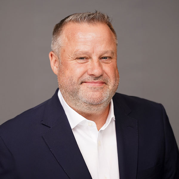
David Haynes
VP Strategic Marketing & Specialty Technologies Strategy, Lam Research Corporation
Bio :
David gained a B.Eng and PhD in Materials Engineering from Swansea University. His PhD thesis was in the field of organic semiconductors for electronic and optoelectronic applications.
In his professional career, David has accrued more than 25 years of experience in the Semiconductor Capital Equipment and research instrumentation sectors. Focused on new technology development, he has a strong process background in plasma etch and deposition for optoelectronics, photonics, MEMS, Power and RF Electronics, as well as advanced chip packaging technologies.
Building on this technical knowledge, David has a proven track record in developing strategic business partnerships, specializing in new technology developments and introduction of enabling process capabilities to leading semiconductor fabs worldwide.
David Joined Lam Research in June 2016. He is currently Vice President of Strategic Marketing in Lam’s Customer Support Business Group and is responsible for Lam’s strategy in Specialty Technologies.
Pioneering Precision Sensing
Pierre-Damien Berger
MEMS Industrial Partnership Manager, CEA-Leti
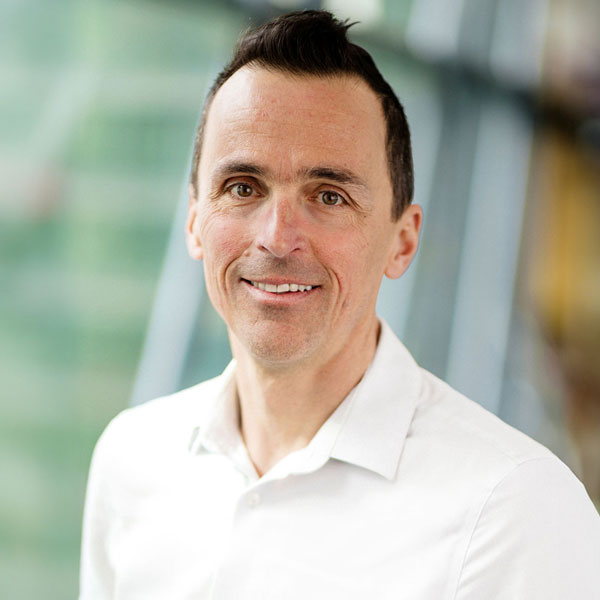
Pierre-Damien Berger
MEMS Industrial Partnership Manager, CEA-Leti
Bio:
Pierre Damien Berger is MEMS Industrial Partnerships Manager at CEA LETI.
CEA LETI is a leading MEMS R&D lab working for industry, with more than 150 people working on these topics – world’s largest MEMS R&D institute.
Pierre-Damien was previously the MinaSmart (European Digital Innovation Hub) director at Minalogic. He worked before as CPS European projects manager, Head of Smart Devices Program, Industrial Partnership Manager and VP Business Development & Communication at CEA-Leti.
With more than 25 years of experience, 10 years in industry, 15 years in R&D serving industry, his experience has allowed him to master the right balance between business and innovation - Understand and listen to needs, identify and select innovative solutions, enhance the functions that meet expectations, communicate to radiate.
Marc Sansa Perna
Project Manager, Optomechanical Sensors Expert, CEA-Leti
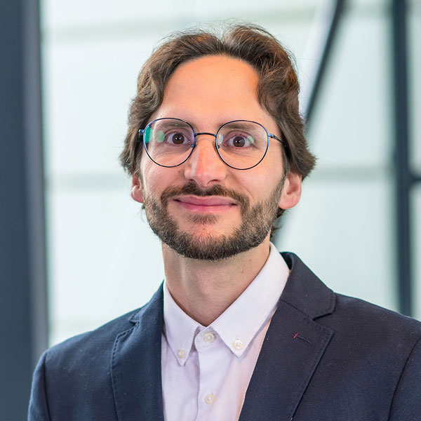
Marc Sansa Perna
Project Manager, Optomechanical Sensors Expert, CEA-Leti
Bio:
Marc Sansa obtained his Ph.D. degree in electronic engineering from the Universitat Autònoma de Barcelona, Barcelona, Spain, in 2013. He is an expert in microelectromechanical system (MEMS) sensors, RF MEMS and optomechanics, having co-authored over 50 publications and several patents. He is currently a project manager at the Sensors and Actuators Laboratory of CEA-Leti.
Marcus Zimnik
EMEA Director of Innovation & Technology, Texas Instruments
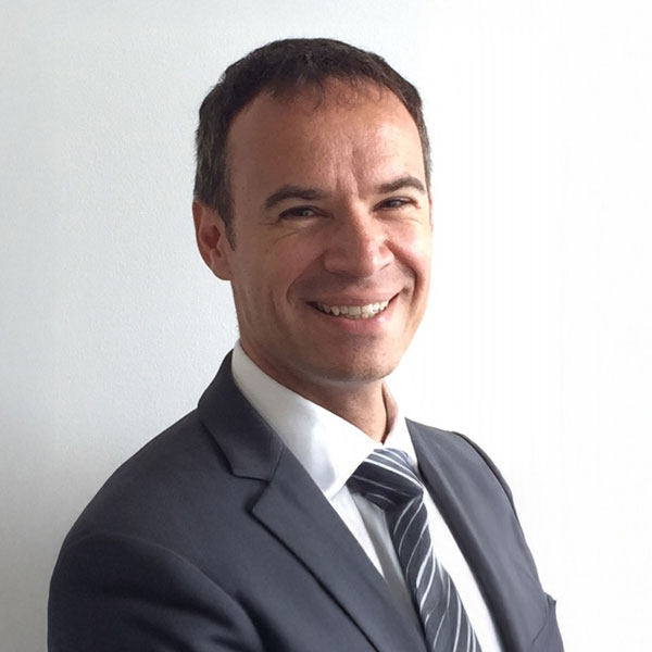
Marcus Zimnik
EMEA Director of Innovation & Technology, Texas Instruments
Bio:
Marcus Zimnik received the Dipl. Ing. in EE from the Technical University of Regensburg and started his career at Texas Instruments in 1998 as a field application engineer. Since then, he held various managing positions supporting TI's key accounts in the automotive, industrial and telecom sectors.
In 2019 he became the EMEA Director of Innovation and Technology. In this role he’s focused on strategic activities to explore new business opportunities and works with strategic customers and partners on new IP and market development.
In addition he leads TI's Innovation Club, an employee network that encourages TI employees to come up with new ideas and put them into action.
Mr. Zimnik has a broad system knowledge and an excellent understanding of various customer applications.
Abstract:
Next generation sensors embed multiple sensing modalities into a single chip, providing more information at a smaller footprint. These sensing devices will be able to sense e.g. multiple gases or substances on a single device reducing the number of sensors needed in a system. Combined with extreme edge AI, the information quality increases while power consumption can be reduced e.g. in wireless sensor nodes. I will share some thoughts on these concepts and how future sensor systems could look like.
Jérôme Mouly
Director of Sensing, Imaging and Display Activity, Yole Group
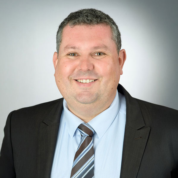
Jérôme Mouly
Director of Sensing, Imaging and Display Activity, Yole Group
Bio:
Jérôme Mouly is Director of sensing, imaging and display at Yole Group.Jérôme manages the expansion of the technical expertise and market know-how of the team. In addition, Jerome’s mission focusses on the management of business relationships with company leaders and the development of market research and strategy consulting activities.He has conducted more than 100 marketing and technological analyses for industrial groups, start-ups, and institutes in the field of MEMS and sensing technologies.Jérôme has been also deeply engaged in Yole Group's finance activities with a dedicated focus on the commercial exploitation of smart system technologies and access to funding opportunities.Jérôme is regularly involved in international conferences, with presentations and keynotes.Jérôme Mouly earned a Master of Physics degree from the University of Lyon (FR).
Abstract:
The MEMS & Sensors industry is at a crossroads, characterized by both resilience and turbulence. Despite experiencing difficult periods in 2023 and 2024, mainly due to a decline in consumer electronics and global economic instability, the outlook for the future is optimistic. In the sensor industry, “high-end” sensor demand is accelerating to serve defense, Industry 4.0 and other harsh environment applications. New development and innovative technologies are at the forefront of the requested performances. The presentation is be an overview of the MEMS and sensor industry trends, identifying the critical factors driving growth, and how technological innovation is reshaping the landscape.
Ivan Favero
Research Director, CNRS, Université Paris Cité
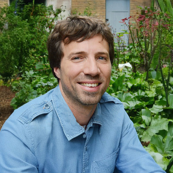
Ivan Favero
Research Director, CNRS, Université Paris Cité
Bio:
Ivan Favero, head of the optomechanics team at Matériaux et Phénomènes Quantiques labs of Université Paris Cité-CNRS. Recipient of ERC Starting 2012 and ERC Consolidator 2018. For more than ten years, the research of Ivan Favero has enabled developing semiconductor nano-optomechanical devices for quantum physics and sensing applications. Along the two ERC projects (NOMADE and NOMLI) his team has set a forefront expertise in the physics, modeling and understanding of optomechanical resonators, as well as in highly sensitive all-optical measurement techniques.
Abstract:
I will discuss our progress in the dual optical and mechanical measurement of liquids on the micron scale. I will focus on situations where optomechanics enables concrete gains in time-resolution and sensitivity, giving access to temporal and spatial scales little explored in the liquid state. A central development is the rheology of microscale volumes of liquids at high-speed, with applications in the industrial and medical sectors.
Mikaël Colin
Head of MEMS Laboratory, CEA-Leti
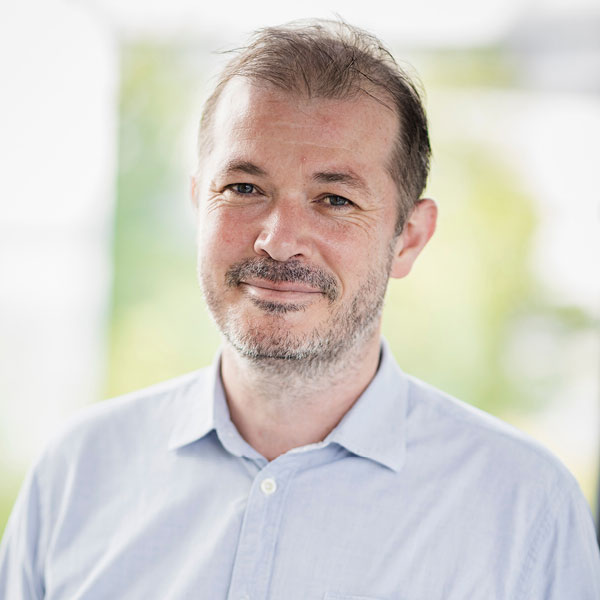
Mikaël Colin
Head of MEMS Laboratory, CEA-Leti
Bio:
Mikaël Colin has been the head of the MEMS sensors and actuators laboratory at CEA-Leti since 2021. With over 20 years of experience in the MEMS field, he began his career in England as a designer of silicon photonic components for telecommunications. Since 2004, he has focused on sensor technologies, working first in industry, then at CNRS, before joining CEA-Leti in 2013. Mikael Colin holds a Master's degree in Optics and a PhD on energy harvesting for cardiac implants.
Abstract:
To continue the deployment of microsystem technologies, or to address new markets where MEMS technologies do not yet meet the needs, one of the main challenges is to constantly improve the precision of sensors. This presentation will highlight some examples of innovations achieved by CEA-Leti, particularly those enabled by technological advancements. We will also focus on the work conducted over several years on optomechanical sensing, which exploits the advantages of this ultra-precise transduction method and opens the door to unprecedented levels of performance in sensors.
Raphael Levy
Head of the Sensors & Micro/Nano Technology Unit, Onera
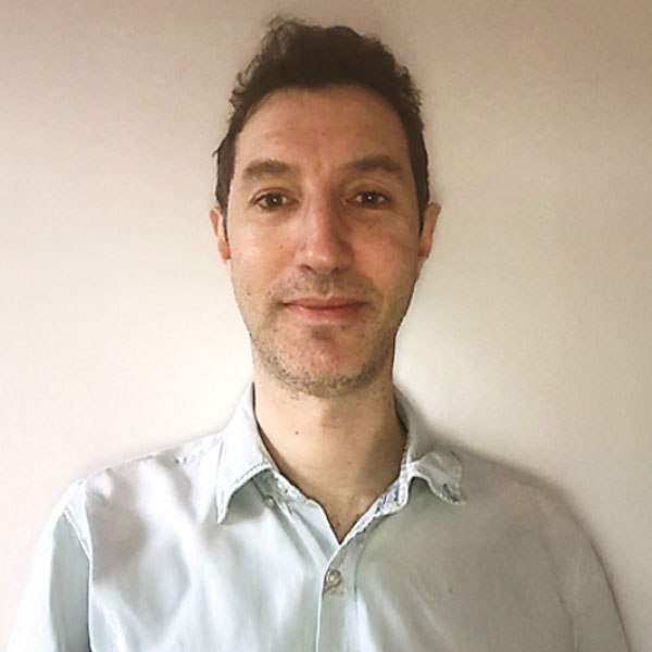
Raphael Levy
Head of the Sensors & Micro/Nano Technology Unit, Onera
Bio:
Raphael Levy is currently at the Head of the Sensors & Micro/nano technology unit at ONERA - The french aerospace lab. His research focuses on high performances MEMS devices based on quartz crystal resonators for high performances miniature sensors dedicated to aerospace applications, and especially Position, navigation and timing devices to adress the navigation grade. He received PhD degrees from the University of Paris-Saclay in electrical engineering in 2005
Abstract:
Quartz resonators have been used for a long time for time and frequency applications, taking advantage of their high frequency stability, high quality factor,and the simplicity of piezoelectric transduction.
These key benefits, together with optimizations concerning transducers analysis and design by FEM simulations and microtechnology process including wet etching, DRIE, and hybrid substrates, allowed to develop high performances devices for PNT (position, navigation, timing) applications (accelerometer, gyroscope, time reference) towards navigation grade, and other sensors including electrostatic field sensor, satellite ion thruster thrust sensor, or photoacoustic gaz sensor.
Franck Badets
Research Director, CEA-Leti
Franck Badets
Research Director, CEA-Leti
Bio:
“ Franck Badets received the MS degree from ENSEIRB, Bordeaux, France in 1995 and a PhD Degree in electronics in 2000 from university of Bordeaux, France. From 2000 to 2011 he was with STMicroelectronics where he supervised a research activity on RF frequency synthesizers and Injection locked oscillators. In 2012 he earned the French accreditation to direct research and joined CEA-Leti. As a research director he currently leads a research activity on cryoCMOS IC design for quantum computing and another on the design of silicon oscillators for sensing and reference frequency applications.
Abstract:
The high quality factor of optomechanical resonators paves the way to the design of ultra-low phase noise reference frequency generators running at several hundreds of MHz up to few GHz. In this presentation we will first focus on the possible applications of optomechanical oscillators. In a second part, we will address the electronic design challenges by presenting two on-going projects at CEA-Leti: a first one intends to design an optomechanical reference frequency for cryogenic applications, while a second one intends to provide a fully integrated CMOS reference generator for consumer applications.
Guillaume Jourdan
Optomechanical MEMS/NEMS Expert, CEA-Leti
Guillaume Jourdan
Optomechanical MEMS/NEMS Expert, CEA-Leti
Bio:
Guillaume Jourdan, a project manager and senior expert at CEA Leti, has been instrumental in advancing optomechanics for nanosensors. With a Ph.D. from the University Grenoble Alpes, he has led innovative projects integrating optomechanical transduction methods at the nanoscale and in particular optomechanical projects implementing ultrafast AFM probes with resonant frequencies up to the GHz range. His work on quantum engineering and sensor applications is currently pushing back the limits of AFM with Optomechanics for ultra-high-speed imaging and quantum sensing.
Abstract:
Over the past 15 years, advances in optomechanics and micro-/nano-fabrication have enabled the development of miniature devices that combine optical cavities with high-quality mechanical resonators. In these systems, strong optomechanical coupling allows for the detection of sub-femtometer displacements at ultra-high frequencies, opening up new technological avenues and experimental windows in Atomic Force Microscopy. This progress paves the way for faster AFM probes with broader bandwidths, enabling ultra-high-speed imaging and nanosecond-scale force spectroscopy to probe molecular biophysics, for example. These advancements also lay the foundation for future quantum AFM and measurements down to the single-phonon level.
Bernard Legrand
Senior researcher, CNRS - LAAS Laboratory
Bernard Legrand
Senior researcher, CNRS - LAAS Laboratory
Bio:
Dr. Bernard Legrand is a Research Director at CNRS, based at LAAS in Toulouse, France. He holds a Ph.D. in Electronics from the University of Lille, France. His research began in semiconductor physics in Lille and later evolved into micro and nanosystems, focusing on MEMS and sensor technologies. At LAAS, he has notably worked on optomechanical Atomic Force Microscopy to open new experimental windows—including GHz AFM probes for high temporal resolution and future prospects toward quantum AFM. With over 120 publications, several patents, and active roles on evaluation and editorial committees, his objective is to develop micro and nanosystems towards new innovative applications beyond conventional uses. Besides optomechanics, his current interests encompass MEMS for adiabatic and neuromorphic computing, as well as chaos-based applications in MEMS resonators, in strong collaboration with MPQ in Paris, and CEA-LETI and TIMA in Grenoble.
Abstract:
Over the past 15 years, advances in optomechanics and micro-/nano-fabrication have enabled the development of miniature devices that combine optical cavities with high-quality mechanical resonators. In these systems, strong optomechanical coupling allows for the detection of sub-femtometer displacements at ultra-high frequencies, opening up new technological avenues and experimental windows in Atomic Force Microscopy. This progress paves the way for faster AFM probes with broader bandwidths, enabling ultra-high-speed imaging and nanosecond-scale force spectroscopy to probe molecular biophysics, for example. These advancements also lay the foundation for future quantum AFM and measurements down to the single-phonon level.
Thomas Alava
Senior Expert - Biological Sensors, CEA-Leti
Thomas Alava
Senior Expert - Biological Sensors, CEA-Leti
Bio:
Dr. Thomas Alava is a staff researcher at CEA-Leti's Heath Division in Grenoble, France. He earned his Ph.D. in micro and nanotechnologies for integrated systems from LAAS-CNRS. His research focuses on developing biosensors, including graphene-based sensors and nanomechanical resonators for mass spectrometry applications. He has co-authored numerous publications and holds several patents in sensor technology. Since 2014, he has been leading efforts in micromechanical biological sensors at CEA-Leti. In 2020, he initiated a program integrating various biosensing technologies into an autonomous vehicle for collecting and analyzing bathing water samples. Thomas Alava work bridges nanotechnology and biotechnology, aiming to advance environmental monitoring and public health.
Abstract:
Water quality monitoring faces a critical challenge: traditional microbiological detection methods are too slow for real-time risk management. The NEO program at CEA-LETI introduces a groundbreaking in-situ biosensing technology, enabling bacterial contamination detection in under an hour. Successfully tested in real-world conditions, this system transforms crisis response capabilities. What are the next steps toward fully autonomous early-warning stations? Join us to explore the future of real-time microbiological monitoring!
Noora Tuomisto
Project Manager, Murata Finland
Noora Tuomisto
Project Manager, Murata Finland
Bio :
Noora Tuomisto started at Murata Finland as a MEMS gyroscope designer and after a couple of years moved on to project management. She has led MEMS projects for automotive customers from R&D to start of production. Her background before Murata is in physics with a PhD on computational modelling of quantum mechanical tunneling in nanoelectronics components.
Murata Finland is a global MEMS Center of the Japanese Murata Group. The company is a leading supplier of MEMS elements and components for applications in automotive, medical, industrial and consumer electronics.
Abstract :
R&D in Murata Finland is focusing on providing products and solutions for the autonomous driving market. Precise localization and operational safety set demanding performance requirements for inertial measurement units. In the future components need to serve multiple automotive systems, e.g. AD/ADAS, chassis control, ESC and safety restraint systems. This will require extreme high performance and functional safety. The talk will provide insight in Murata’s unique MEMS technology and innovative 3-axis sensor concepts behind our new High Performance 6 DOF Sensor product, SCH1633.
Quentin Josso
R&D Director - Technological Research Infectious Diseases, bioMérieux
Quentin Josso
R&D Director - Technological Research Infectious Diseases, bioMérieux
Bio :
Quentin Josso is an engineer-physicist specializing in IVD technologies. He joined bioMérieux in 2012 to manage collaborative research projects dedicated to ultra-fast microbiology in the joint CEA-bioMérieux team. He then took charge of a team of multidisciplinary researchers dedicated to upstream projects within bioMérieux's R&D unit. The work carried out covers a wide range of disciplines and demonstrated proof-of-concept projects from ideation to demonstrations on clinical samples, using a variety of technologies including artificial intelligence, imaging, spectrometry and sample preparation.
Abstract:
Recent evolutions in healthcare systems and related constraints, exacerbated by the SARS-CoV-2 pandemic, have catalyzed a shift towards near-patient testing. Maintaining performance standards equivalent to gold-standard methods across various use cases remains essential. This presentation will address some current challenges, including sample preparation, signal amplification, and read-out mechanisms and some proposed technological solutions will be discussed.
Philippe Robert
CEO, iNGage
Philippe Robert
CEO, iNGage
Bio :
Philippe Robert is CEO and co-founder of iNGage, a deeptech startup developing a new generation of high-performance MEMS sensors. He holds a PhD in Microtechnologies and began his career at the startup SILMAG, developing advanced magnetic sensor technologies for data storage, before joining THALES to work on high-end MEMS inertial sensors for aerospace and defense applications.
He joined CEA-Leti in 2001, where he held successive leadership roles, including Head of the MEMS Sensors Laboratory and Head of the Microsystems Department (120+ people), before leading Business Development for Microsystems.
In 2025, he founded iNGage as CEO & CTO, leading corporate strategy, fundraising, and execution.
He has authored over 50 scientific publications and holds more than 60 patents, including more than 20 related to the M&NEMS architecture at the core of iNGage’s innovation.
Hamidreza Neshasteh
Research Engineer, CNRS, Université Paris Cité
Hamidreza Neshasteh
Research Engineer, CNRS, Université Paris Cité
Bio :
Hamidreza Neshasteh is a research engineer at the Matériaux et Phénomènes Quantiques laboratory of Université Paris Cité-CNRS, currently leading the creation of a spin-off. After completing his PhD in 2023 on optomechanical sensors as part of the ERC NOMLI project, he joined technology maturation projects supported by CNRS and ERC PoC programs. His work focuses on developing a post-fabrication tuning process for photonic chips with picometer-level precision, targeting applications in advanced photonics and optomechanical sensing.
Jean-Michel Jurine
Senior Operations Manager, Rakon France

Jean-Michel Jurine
Senior Operations Manager, Rakon France
Bio :
Graduate of the Physics school of Grenoble, Jean-Michel JURINE has developped and run as manager different product lines in semiconductor probe cards applications, aircraft parts engine and finally in Quartz Oscillators for telecom, Military and Space usages.
Abstract :
Quartz application in timing has reach a very high level of performance, competing with atomic clocks on the very short term. Considered as a commodity product in most consumer or industrial applications, bringing those high perfomance to volume manufacturing is the next challenge of Quartz or similar solutions to enable new usage for Precise Timing and Navigation.
Thomas Rodgers
Senior Director, Head of Electronics Business Sector, ZEISS Microscopy
Thomas Rodgers
Senior Director, Head of Electronics Business Sector, ZEISS Microscopy
Bio :
Thomas Rodgers leads the electronics business sector at ZEISS Microscopy, a team responsible for defining the market and portfolio strategy for ZEISS' microscope products and solutions toward the semiconductor industry.
Prior to joining ZEISS, Thomas worked in a variety of technical and commercial roles within Roper Scientific's Princeton Instruments business (now part of Teledyne). Most recently, he was their country manager for Japan.
Thomas studied Electrical and Electronics Engineering and Applied Physics at Swinburne University in Melbourne, Australia, completed a PhD in Applied Physics from Osaka University in Japan, and also holds an MBA from IMD Business School in Lausanne in Switzerland.
Abstract :
We review the recent advances of advanced microscopey applications for the semiconductor laboratory.
While microscopy using electrons, light or xrays has been used in semiconductor physical analysis for decades, recent trends in semiconductor technology present new analysis challenges which require new analysis technology, or the revival of microscopy techniques that have long been underused in the semiconductor context. We present an overview of microscopy methods of recent interest - in the context of semiconductor failure analysis applications.
The FAMES Pilot Line
Dominique Noguet
FAMES Pilot Line Project Coordinator, CEA-Leti
Dominique Noguet
FAMES Pilot Line Project Coordinator, CEA-Leti
Bio:
Dominique Noguet holds an engineering degree of the National Institute of Applied Sciences (INSA) in electrical engineering in 1992, and a PhD from National Polytechnical Institute of Grenoble (INPG) in 1998. Then, he held several positions at CEA-Leti as a digital IC designer, lab manager and department manager. He led many projects at a national level and in several European frameworks (FP5, FP6, FP7). In January 2023, he was appointed project manager for the France 2030 flagship project NextGen. He is currently the coordinator of the FAMES Pilot Line and reports to CEA-Leti’s CEO. Dominique is a CEA senior expert and an IEEE Senior Member. He has authored or co-authored ~100 scientific papers (several best paper awards), several book chapters and 15 patents. He was a reviewer and a member of scientific committees of many conferences and a member of journal editorial boards. He was conference chair and TPC chair of several international conferences.
Abstract:
The FAMES pilot line has reached a pivotal stage, with highly innovative results obtained on all developed technologies.
These outcomes enable to strengthen FAMES partnerships and further feed other FAMES key initiatives, such as our
open-access and training programs. Moreover, the official inauguration of the Pilot Line earlier this year, was marked by the
launch of a state-of-the-art cleanroom, which is a major asset of the Pilot Line implementation strategy.
Abstract:
The goal of this presentation is to introduce the FAMES project and explain the technologies that have been developed. It will also explain how to use the FAMES pilot line, which can be accessed in various ways, including the open access mechanism. Finally, it will briefly introduce this first technical workshop and the future actions expected throughout the project.
Susana Bonnetier
FAMES Pilot Line Open Access Chairperson, CEA-Leti
Susana Bonnetier
FAMES Pilot Line Open Access Chairperson, CEA-Leti
Bio:
Susana Bonnetier is a member of the FAMES Pilot Line management team and leads the Open Access effort with the goal of making « European-grown » advanced semiconductor technologies readily accessible to industry and academia.
An MIT engineer with a background in industry and research in the USA and France, Susana puts all her energy into transferring technological innovation to companies.
Born in Venezuela, Susana spent 9 years in the USA, where she completed her higher education and worked for General Electric Aircraft Engines, designing and building aircraft engines.
In 1991, Susana joined Saint-Gobain in France, first in the Industrial Strategy and Planning department working with 20 manufacturing plants to streamline and modernize their operations, and then at Saint-Gobain Cristaux et Détecteurs as Product and Industrial Market Manager, significantly increasing the profitability of a scintillation detectors product line.
In 2001, she moved to Grenoble, “the land of nano and micro technologies”, and reoriented her career towards the semiconductor industry. She joined Freescale as R&D Engineer and contributed to the successful development of the 65nm and 45nm CMOS technology nodes by the Crolles 2 Alliance.
In 2007, Susana joined CEA-Leti, first as head of a joint laboratory between Leti and a major French optics company, and later as Leti’s Carnot program manager, piloting a 14M€ R&D budget within Leti’s Scientific Directorate. During that time, she was VP of the Carnot Network and a member of its board of directors.
Susana brings a solid industrial and R&D experience to the FAMES Pilot Line project and the aim of contributing to the construction, in concert with the FAMES European Partners and the complementary Chips Act Pilot Lines, of a pan-European semiconductor ecosystem with the best Europe has to offer in microelectronics technologies.
Abstract:
The open-access concept of the FAMES pilot line project continues to be a key annual meeting point.This presentation will assess the responses to the 2025 call for proposals, introduce newly opened topics for 2026, and outline participation pathways. It will also feature a dedicated focus on the availibility of pathfinding design kit to evaluate the performance of the 10nm FD-SOI CMOS technology.
Laurent Fesquet
Deputy DIrector of the TIMA Laboratory (UGA - Grenoble INP - CNRS)
Laurent Fesquet
Deputy DIrector of the TIMA Laboratory (UGA - Grenoble INP - CNRS)
Bio:
Laurent FESQUET received the Ph.D. degree in electrical engineering from
Paul Sabatier University, Toulouse, France, in 1997. In 1999, he joined the Grenoble Institute of Technology, Grenoble, France, as an Associate Professor at ENSERG (now PHELMA).
His current research at the TIMA Laboratory today covers asynchronous circuit design, computer-aided design (CAD) for event-based systems and non uniform signal processing. He has served as general and program chair of several international conferences. He is currently the Deputy Director of the TIMA laboratory and CIME Nanotech, an academic center supporting microelectronic teaching and research activities
Abstract:
FAMES includes a dedicated training work package to train engineers and technicians with the skills to leverage FD-SOI technology and design circuits using advanced setups. The FAMES pilot line aims at developing new technological nodes, such as 10 nm and beyond, enabling European companies to create innovative IPs for cutting-edge applications. However, the success of the project hinges on having skilled professionals. Therefore, it is imperative for European company employees and talented microelectronics graduates to acquire specialized knowledge and expertise in FD-SOI technology design and characterization.
Thierry Poiroux
Head of the Characterization, Design and Simulation Department, CEA-Leti
Thierry Poiroux
Head of the Characterization, Design and Simulation Department, CEA-Leti
Bio:
Thierry Poiroux received the M.S. degree in 1995 and the Ph.D. degree in 2000. He joined CEA–Leti as a Research Staff Member in 2000. Until 2002, he was involved in partially and fully depleted silicon-on-insulator (SOI) process integration and compact modeling. From 2002 to 2010, he worked on advanced device architectures and was in charge of multiple-gate device modeling, planar double gate process integration and fabrication of graphene-based transistors. In 2011 and 2012, he has been the Head of the Innovative Device Laboratory of CEA–Leti, dedicated to the development of advanced CMOS technologies. From 2012 to 2018, he developed the second version of the L–UTSOI compact model, selected by the Si2 Compact Model Coalition as a standard industrial model for fully-depleted SOI technologies. From 2018 to 2021, he was the head of the Simulation and Compact Model Laboratory of CEA–Leti, and since 2021, he is in charge of the Characterization, Design and Simulation Department. He has authored or coauthored five book chapters and about 190 papers and communications, and he is author or co-author of about 20 patents.
Abstract:
The presentation will review the physical specificities of FD-SOI transistors, highlighting analogies and differences with respect to bulk transistor behavior, and we will explain how to take advantage of this technology to design performant circuits.
Claire Fenouillet-Beranger
Project Manager, CEA-Leti
Claire Fenouillet-Beranger
Project Manager, CEA-Leti
Bio:
Claire Fenouillet-Béranger joined CEA-Leti, Grenoble, in 1998 where she carried out her PhD. work on the integration and characterization of SOI devices. From 2001 to 2013 she worked as a CEA-Leti assignee in advanced R&D STMicroelectronics center, Crolles, France on FD-SOI (Fully-depleted SOI) technology platform development and characterization. From 2013 to 2020 she worked as the project leader of the low temperature MOSFETs development for 3D sequential integration. From January 2020 to January 2022, she was the LETI SiC pilot line project manager in the frame of the joint development program between SOITEC & AMAT. She is the author and co-author of more than 200 publications in major conferences and journals and of more than 40 patents. She was the co-recipient of the Grand Prix du Général Ferrié in 2012 for her work on FD-SOI. She is in charge of CMOS patent portfolio. Since 2022, she is director of research, and CEA Fellow expert, and co-project manager of the FD-SOI next generation node integration at CEA-Leti.
Abstract:
In the context of 10 nm FD-SOI technology development, new architectural and process building blocks must be implemented to meet the targeted device performance specifications. Strain engineering remains one of the primary performance boosters. Strain can be introduced either at the wafer level or at the device level. Additional process modules are required to further reduce access resistance and enhance overall device performance. In particular, the integration of in-situ doped, faceted raised source and drain regions is critical. Achieving the aggressive contacted poly pitch (CPP) target of 68 nm necessitates the implementation of advanced patterning techniques, specifically Self-Aligned Double Patterning (SADP), to meet density scaling requirements. In this presentation, we’ll dive into each of these levers and explore how they can push FD-SOI to the next level.
Gabriel Pares
Project Manager, CEA-Leti
Gabriel Pares
Project Manager, CEA-Leti
Bio:
Gabriel Parès has an Engineer degree in “material science” from l’Institut National des Sciences Appliquées (INSA) de Lyon, France and a postgraduate degree in “semiconductor material sciences” from the University of Lyon.
He has been working for 32 years in semiconductors and MEMS industry in industrial and R&D fields, formerly for STMicroelectronics and MEMScap, then he joined CEA-leti in 2004.
He is currently project leader at CEA-Leti in the Laboratory of Memories and Computing in charge of the workpackage dedicated to embedded Non Volatile memories of the FAMES pilot line.
Abstract:
The presentation will address embedded Non-Volatile Memory (eNVM) devices integrated in the BEOL of advanced CMOS technologies starting from the 22nm and going towards the 10 and 7nm FD-SOI technology nodes. One of the goals of eNVM in the framework of FAMES is to open opportunities for disruptive IC architectures and designs using the most appropriate eNVM for the considered applications and use cases. OxRAM, FeRAM, BEOL FeFET and MRAM will be addressed in the presentation. Exploration of potential new applications will cover mainstream domains such as Artificial Inteligence and security for instance.
Somnath Pal
Scientist, Silicon Austria Labs
Somnath Pal
Scientist, Silicon Austria Labs
Bio:
I am Dr. Somnath Pal, a passionate researcher with a Ph.D. in Materials Science, specializing in engineering magnetic, high-κ dielectric, and multiferroic materials. My expertise lies in semiconductor device design, modeling, and microfabrication, with hands-on experience in thin film deposition techniques such as sputtering, e-beam evaporation, ALD, and PECVD. I have a strong background in photolithography, including e-beam lithography, and ICP/RIE etching processes. My skills extend to advanced microscopy techniques like SEM/EDS, FIB, AFM, and optical spectroscopy. I am well-versed in electrical characterization of fabricated devices, including IV, CV, and VNA measurements. Additionally, I have proficiency in simulation and statistical tools such as COMSOL, MATLAB, LabView, JMP, and Minitab. My research interests focus on RF MEMS development, particularly Piezo MEMS resonators, with the goal of advancing next-generation microsystems. Recently, I joined Silicon Austria Labs as a Scientist, contributing to the advancement of Magnetic Microsystems Technologies.
Abstract:
An RF circulator is a non-reciprocal, three-port passive device that enables directional signal flow between ports, ensuring isolation between transmit and receive paths. Traditional circulators depend on ferrite materials with external magnetic biasing, which limits integration and scalability. To address this, we focus on CMOS-compatible circulator designs utilizing barium hexaferrite (BaM) thin films for self-biasing, eliminating the need for bulky magnets. This talk presents the design, fabrication, and characterization of a self-biased RF circulator, emphasizing material selection, deposition techniques, and challenges in achieving uniform film quality and miniaturization. The characterization includes S-parameter analysis (S11, S21, S31) to assess insertion loss, isolation, and return loss.
We are fabricating and integrating these CMOS-compatible circulators for the FAMES pilot line, aiming to develop scalable, cost-effective, and high-performance RF circulators for next-generation wireless technologies.
Emmanuel Ollier
Program Manager, CEA-Leti
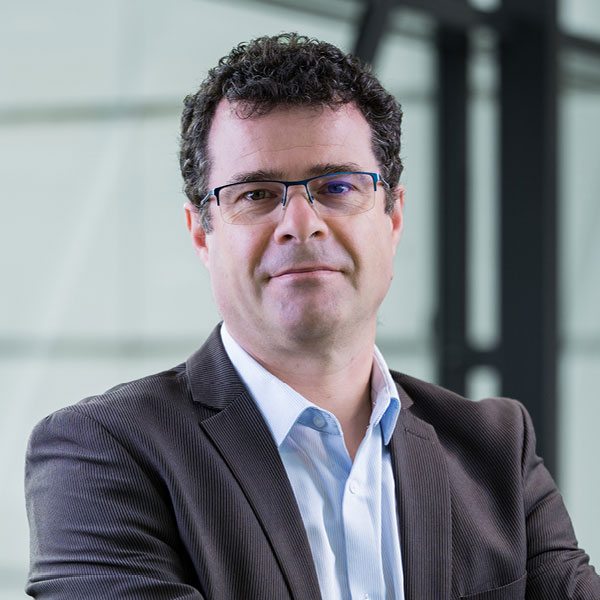
Emmanuel Ollier
Program Manager, CEA-Leti
Bio:
Emmanuel Ollier is Program Manager in the Silicon Components Division of CEA-Leti. During the last 4 years, he headed the 3D Integration Technologies Laboratory of CEA-Leti, specialized in heterogeneous integration for high-performance computing & AI, RF communications, IoT and power. He previously worked in technology development at NXP (Crolles2 Alliance) on logic nodes, at ATMEL on embedded flash memories, and THALES on MEMS. He holds 22 patents and has authored 45 papers and communications in international conferences. He holds an engineering degree in Physics and Chemistry from the Ecole Nationale Supérieure de Chimie et Physique of Bordeaux, France and a Ph.D. in materials sciences from the University of Compiègne, France.
Abstract:
Since ITRS became IRDS in 2017 to follow the trend of microelectronic system integration, heterogeneous integration technologies and system architectures have undergone major revolutions. The SoC (System–on-chip) architectures are now evolving towards Chiplet architectures. Functions are partitioned into different chips to take advantage of the best of each technology and reduce time to market. Not only does this approach affect technology development and manufacturing, but it also transforms interactions and business models. This presentation will show how CEA-Leti and the FAMES pilot line are at the forefront of innovation in this area, especially on technology challenges and computing and RF applications.
Cian Ó Mathúna
esearch Program Director, Integrated Power and Energy Systems, Tyndall, Tyndall National Institute
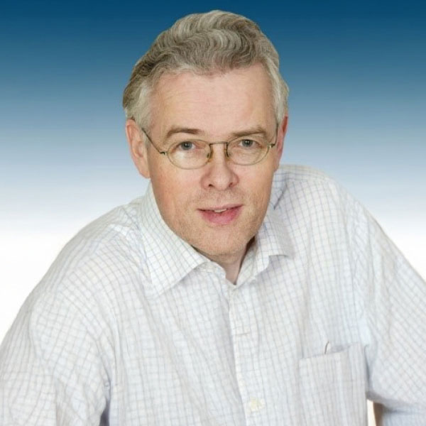
Cian Ó Mathúna
esearch Program Director, Integrated Power and Energy Systems, Tyndall, Tyndall National Institute
Bio:
Cian Ó Mathúna's research, on the miniaturisation and integration of magnetics onto silicon (MagIC - making magnetics disappear onto silicon), has contributed to disruptive developments in integrated power management for processors in portable and high performance computing and to the commercailisation of magnetics-on-silicon in portable computers. In 2008, he founded the International Workshop on Power Supply on Chip (PwrSoC), a flagship event for IEEE PELS and PSMA. An IEEE Fellow, he has received an IEEE PELS Technical Achievement Award for Integration and Miniaturisation of Switching Power Converters and an EARTO (European Association of Research and Technology Organisations) Impact Innovation Award.
Abstract:
Magnetics-on-silicon (MagIC - making magnetics disappear onto silicon) has been a key enabler in the emergence of integrated power management and vertical power delivery for microelectronic systems. This talk will introduce the technology and its associated performance capabiities. The talk will also introducre the development of micro-transfer printing of chiplets (i.e. PMICs, micro-inductors on silicon and high denisty trench capacitors) to enable the heterogeneous integration of individual and granular arrays of miniaturised dc-dc converters for high efficiency, integrated power delivery.
Cédric Rolin
Program Manager, Imec
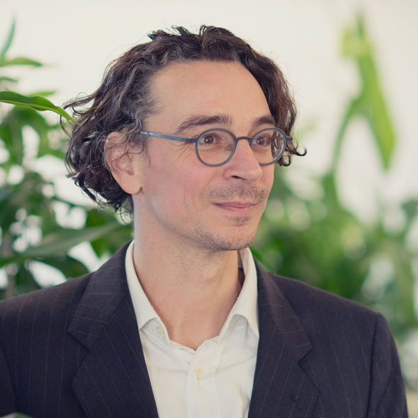
Cédric Rolin
Program Manager, Imec
Bio:
Cédric Rolin is Manager for the Sustainable Semiconductor Technologies and Systems (SSTS) Program at imec. After more than 15 years spent both at imec and at University of Michigan holding various positions as researcher and team leader in the fields of large-area flexible electronics and nanoimprint lithography, Cédric has joined in 2021 the sustainability team of imec as Program Manager, focusing on the assessment and improvement of the environmental footprint of the semiconductor manufacturing industry.
Abstract:
This presentation will cover the research activities carried out by the Sustainable Semiconductor Technologies & Systems (SSTS) program at imec in the context of the sustainability work package 11 of the FAMES project. We develop life-cycle assessment models for the environmental footprint of manufacturing integrated circuit chip in a high volume fab, covering a broad range of technologies (logic, memory, RF, advanced packaging, etc.). The same approach can be downscaled to module or even single process step level, enabling the calculation of an environmental E-score that is used to guide eco-innovation in semiconductor processing and flow integration. Such E-score is instrumental in the selection and evaluation of fab research projects aiming at the development of more sustainable semiconductor processes.
Dr. Sambuddha Khan
Tyndall
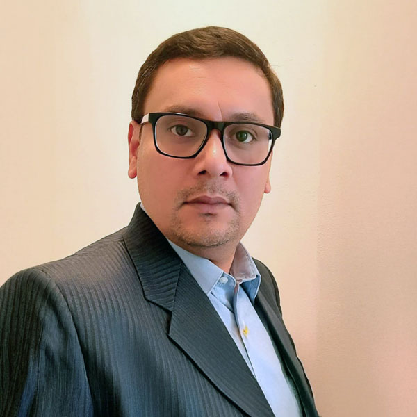
Dr. Sambuddha Khan
Tyndall
Bio:
Dr. Sambuddha Khan is an experienced researcher specializing in advanced ICT materials, Microfabrication processes, and MEMS devices, with extensive expertise in Heterogeneous Integration. With over a decade of post-PhD experience, his research encompasses Advanced Microfabrication techniques, MEMS packaging, Piezoelectric-based RF MEMS, Inertial MEMS, and bio-MEMS. Currently serving as a Senior Scientist at Tyndall National Institute, Dr. Khan leads the Integration of Power Management Components activities within the FAMES Pilotline Project. He has a strong track record of managing several government and industry funded projects in the area of MEMS and advanced packaging.
His primary research interests focus on integrated magnetic devices for power conversion, scandium-doped Aluminium Nitride (ScAlN)-based piezoelectric RF resonators, and innovative heterogeneous integration methods for next-generation on-chip power supply. Beyond his research role, Dr. Khan actively contributes to academia as a lecturer in MEMS and Microfabrication at University College Cork (UCC), where he is committed to mentoring and fostering collaboration with the next generation of scientists advancing cutting-edge MEMS technologies.
Abstract:
Angeline Tee
Senior Manager, Strategic Planning, Silicon Austria Labs
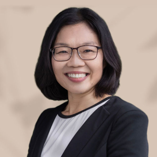
Angeline Tee
Senior Manager, Strategic Planning, Silicon Austria Labs
Bio :
Angeline Tee has over 25 years of global experience in MEMS and microelectronics. At Silicon Austria Lab (SAL), she supports the Microsystem Division in business strategy and planning and oversees the execution of its strategic partner engagements. As the division actively participates in several EU Chips Act pilot lines hosted at SAL, she also coordinates internal alignment to ensure smooth implementation and delivery of pilot-line activities with external stakeholders.
Prior to joining SAL, Angeline held roles at GLOBALFOUNDRIES, X-FAB MEMS Foundry, and A*STAR’s Institute of Microelectronics, where she focused on market research, industrial collaboration, and partnership development to drive growth and sustainability.
Lucille Engels
COO & cofounder, IC'Alps
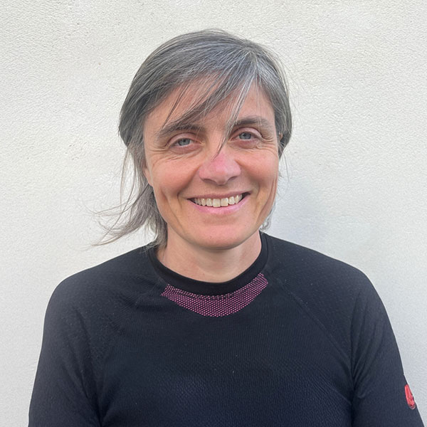
Lucille Engels
COO & cofounder, IC'Alps
Bio :
Lucille Engels received the M.S. degree in electrical engineering from the National Polytechnic Institute of Grenoble, France, in 1999. She started at Dolphin Integration as a design engineer for silicon IP, evolved as project manager and ASIC team leader. She co-founded IC’Alps in 2018 to design custom ASIC for diverse applications, currently working with her technical team to develop skills in ultrasounds, ultra-low power designs, power management and sensor interfaces.
Abstract :
Karl-Magnus Persson
Project Manager & Senior Scientist, VTT
Karl-Magnus Persson
Project Manager & Senior Scientist, VTT
Bio :
Dr Persson received his M.Sc. degree in engineering nanoscience, and later, his PhD in electrical engineering, from Lund University, Lund, Sweden, in 2008 and 2014, respectively. After graduation he pursued two consecutive postdoctoral fellowships at Stanford University, Stanford, USA, 2015-2017, and Lund University, 2017-2020, focusing on devices and circuits for non-volatile resistive memories (NVM). In 2021, Dr Persson joined the Finnish research institute, VTT, Espoo, Finland, where since 2024 he is the VTT project manager for EU FAMES, overseeing the infrastructure investments and pilot-line research and development efforts.
Hervé Ribot
Director, Micro-Nanoelectronics & Quantum technologies, in charge of the “Asteerics” Competence Center, Minalogic
Hervé Ribot
Director, Micro-Nanoelectronics & Quantum technologies, in charge of the “Asteerics” Competence Center, Minalogic
Bio :
Hervé RIBOT holds a PhD in Optics, Optoelectronics and Microwaves from Grenoble INP. After working in industrial R&D at IBM, Alcatel, and Philips, he joined the U.S. startup Alphion in 2001, focusing on all-optical regeneration.
He joined CEA-LETI in 2006, leading teams in 3D integration, packaging, and power devices, and later moved to CEA-IRIG to support the industrial transfer of advanced research, with main focus on spintronics and quantum technologies.
Today, he is Technical Director for Micro-Nanoelectronics and Quantum at Minalogic, helping members access public funding for ambitious R&D and leading the Asteerics Competence Center to promote high-efficiency ASICs using FDSOI, GaN, and SiC.
Sana Ibrahim
Research Engineer in Microelectronics Design, Grenoble INP
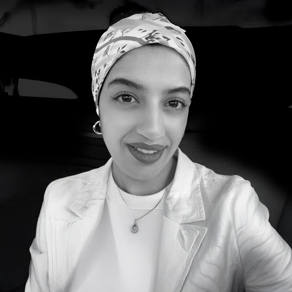
Sana Ibrahim
Research Engineer in Microelectronics Design, Grenoble INP
Bio :
Sana Ibrahim received the M.S. degree in Wireless Integrated Circuits and Systems from Grenoble Alpes University (UGA), Grenoble, France, in 2020, and the Ph.D. degree in Nanoelectronics and Nanotechnologies from TIMA Laboratory, UGA, Grenoble, France, in 2024. In 2025, she joined Grenoble Institute of Technology (INP), Grenoble, France, as a research engineer at Phelma within the European project FAMES. During her doctoral studies, her research focused on the design of a wideband, low-power RF front-end based on N-path mixers in 28nm FD-SOI technology.
Her current work involves on developing and contributing to a comprehensive curriculum covering both analog/RF and digital design flows, aimed to provide designers with the foundational knowledge needed to develop integrated circuits using FD-SOI technology.
Jari Kinaret
Executive Director, Chips Joint Undertaking
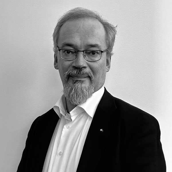
Jari Kinaret
Executive Director, Chips Joint Undertaking
Bio:
Jari Kinaret was born in Finland and holds M.Sc. degrees in Theoretical Physics and Electrical Engineering from the University of Oulu in 1986 and 1987, respectively, and a Ph.D. in Physics from the Massachusetts Institute of Technology (MIT) in 1992.
Prof. Kinaret has worked in various roles at research institutes and universities in Copenhagen, Denmark, and Gothenburg, Sweden. From 2013 to 2023, he served as the Director of the Graphene Flagship, a one-billion-euro research project dedicated to exploring the potential of graphene.
In October 2023, Prof. Jari Kinaret assumed the role of Executive Director at Chips Joint Undertaking (Chips JU), a European public-private partnership that supports research, development, innovation, and future manufacturing capacities in the European semiconductor ecosystem.
AI Transforming HPC & Data Centers
Jean-Philippe Bourgoin
Deputy Executive Director of the Technological Research Division, CEA
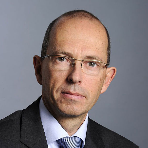
Jean-Philippe Bourgoin
Deputy Executive Director of the Technological Research Division, CEA
Bio:
Deputy executive director of the Technological Research Division (4500p, 650M€/y) at the French Alternative Energies and Atomic Energy Commission (CEA).
Co-leader of CEA’s quantum technologies program and acting co-pilot of the national priority research and equipment program on quantum technologies.
From June 2017 to august 2019 and may to December 2020 he was senior advisor for research, innovation and industry at the cabinet of Professor Frédérique VIDAL, Minister for higher education, research and innovation in President Macron Government.
From January 1st 2016, to May 2017, he was director for Strategic analysis, member of the CEA executive committee after he had been appointed corporate Strategy and Programs Director in 2011 and Nanoscience Program Director in 2006. He was President of the High Performance Computing and Simulation steering committee at CEA 2016-2017 and the secretary of the Atomic Energy Committee 2010-2015.
He represented France in various international missions related to nanotechnology (OECD, High Level Groups, Japan-France FOE, EU-US coordination on nanotechnology…) and was expert for various national, EU and international funding agencies and programs.
He was a member of the boards of Genci (French supercomputing agency), Soleil Synchrotron, Ecole normale supérieure Paris-Saclay, Paris-Sud University...
He was President of the Micro-nano sectorial scientific committee of the National Research Agency (ANR) and contributed to the development of nanotechnologies in France.
He was head of the CEA Molecular Electronics Laboratory (2001-2008), co-founder and head of the joint CEA-Motorola Molecular Electronics Laboratory (2001-2003), deputy manager of the Service de Physique de l'Etat Condensé (2005-2006).
He studied at Ecole Normale Supérieure Paris-Saclay , received a Ph.D. in Physical-Chemistry from Paris-Saclay University in 1991, did his post-doc with Dr H. Rohrer (Nobel Prize) and Dr B. Michel at IBM Rüshlikon in 1993-1994 and was delivered an Habilitation in solid state physics in 2001. His science and technology interests include nano and quantum devices, advanced nanoelectronics, nanomanufacturing, material sciences, information theory, new architectures of computation and AI, supercomputing. He published more than 100 scientific publications, cited ~3700 times (H-index=34), gave more than 75 invited conferences and obtained 12 patents.
He is Knight of the Ordre National du Mérite.
Abstract:
Julie Galland
Director of the Technological Research Division, CEA
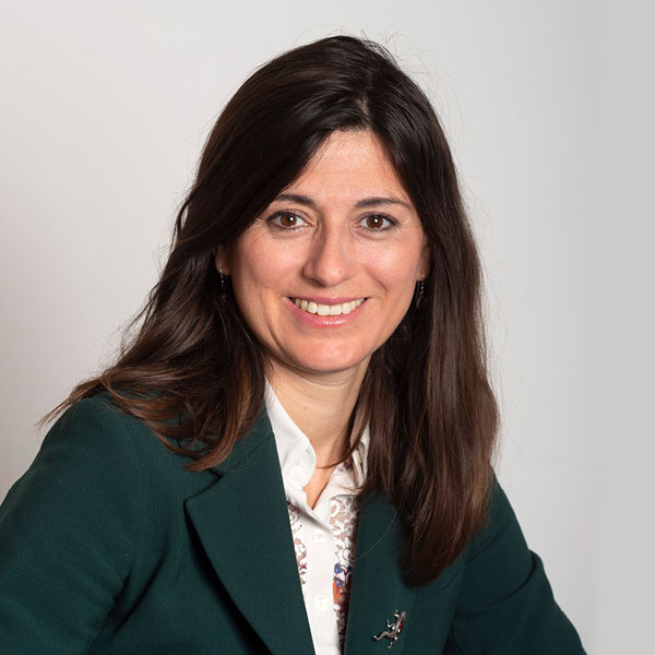
Julie Galland
Director of the Technological Research Division, CEA
Bio :
Director of Technological Research at the CEA since January 2023, Julie Galland is a graduate of the École Polytechnique (Palaiseau, France), and holds a doctorate in solid state physics.
At the CEA, she leads the Technological Research division of about 3500 Employees who develop key enabling technologies that foster the competitiveness of national and european industry, and contribute to solve the major challenges posed by the necessary energy transition, the advent of digital technology and demographic upheaval.
Before joining the CEA, Julie Galland held a number of positions within the French ministry of economic affairs between 2012 and 2023. First as head of the office in charge of the Semiconductor Sector and then of the office in charge of the Health Industries Sector, Julie Galland most recently held the position of Deputy Director for the Aerospace, Electronics and Software Sectors, where she drew up research, development and industrialisation policies. Julie Galland has been responsible for structuring projects to promote innovation and productive investment in the fields of semiconductors, pharmaceuticals and medical devices, the cloud, HPC and space. In these sectors, she has contributed to the structuring of industries and the consideration of public policy guidelines.
Abstract :
Arnaud Lépinois
Group CEO, Eclairion
Arnaud Lépinois
Group CEO, Eclairion
Bio :
Arnaud has held various leadership roles in technology companies such as HP, Computacenter, Neurones, and IBM. As an entrepreneur and intrapreneur, he has also founded several international companies. Before joining HPC, Arnaud Lépinois served as the Director of Transformation and Group CIO (Excom member) at CMA CGM. A a former professional athlete, he began his career in 1996 at IBM as an engineer and product manager. In 2000, he became the Chief Technology Officer of the Inexware Group, which was acquired by the Neurones Group in 2002. In 2005, he relocated to Canada and founded several companies in various fields, including audiovisual production for film, television, and the web; mobility solutions development; biotechnology; and fintech. Upon his return to France in 2012, he became the Director of Managed Services at Computacenter, eventually taking over as CEO in 2017. In 2020, he became the President and CEO of HP Inc. France, leading the organization’s transition toward services. His industrial experiences, expertise in IT infrastructure, understanding of major outsourcing contracts, and new technology consumption models enable him to effectively and successfully support organizations in their transformation. Arnaud is a graduate of the INSA Lyon with a degree in Industrial Engineering.
Abstract :
The AI Infrastructure Factory represents a complete reinvention of datacenter design and operation, purpose-built to meet the technical requirements of the new generation of high-performance and AI machines. Unlike traditional datacenters, it is designed from the ground up to support extreme compute density, direct liquid cooling (DLC), and modular scalability, ensuring optimal performance, energy efficiency, and sustainability. This new model breaks away from legacy constraints to provide an infrastructure truly adapted to the power, cooling, and integration needs of today’s and tomorrow’s most demanding workloads.
Ian O’Connor
Professor, Ecole Centrale de Lyon
Ian O’Connor
Professor, Ecole Centrale de Lyon
Bio :
Ian O'Connor is Distinguished Professor for Heterogeneous and Nanoelectronics Systems Design at Ecole Centrale de Lyon, France, joint head of the Electronics group at the Lyon Institute of Nanotechnology, and Director of the SoC2 research network. His research interests include novel computing and interconnect architectures using emerging technologies and design exploration methods. He has authored or co-authored over 300 book chapters, journal publications, conference papers, and patents, held key roles in organizing international conferences, and led several national and European projects. He serves as an expert with IRDS Systems and Architectures, IFIP WG10.5, is Vice-President for Technical Activities in IEEE CEDA, Vice-Chair of the EDAA Main Board, and Associate Editor for IEEE Transactions on Computer-Aided Design of Integrated Circuits and Systems and IEEE Transactions on Circuits and Systems for Artificial Intelligence.
Abstract :
As artificial intelligence and large language models accelerate datacenter progress, hardware must address intensifying power and energy constraints, sustainability requirements, and the complexity of scaling operations while integrating diverse specialized hardware. We are already seeing a surge in accelerator-rich architectures aimed at reducing latency for real-time applications, deploying specialized and heterogeneous hardware for better power efficiency, and building scalable clusters to support thousands of concurrent agents. This talk explores emerging trends such as in-memory computing to reduce data movement costs, the adoption of chiplets and 3D integration, and fine-grained dynamic reconfigurability for model tuning and anti-obsolescence. It will conclude with a look at the long-term prospects of analog computing and the advantages of photonics for interconnects and in-network computing.
Sébastien Cruz-Mermy
Data Center innovation & Tech Explore league leader, Schneider Electric
Sébastien Cruz-Mermy
Data Center innovation & Tech Explore league leader, Schneider Electric
Bio:
I joined Schneider Electric in 2008 as part of the international project center team leading large projects development mostly in renewable energy and mission critical facilities where I performed technical and business development roles.
In 2013, I took a Global Service Sales role with the responsibility to develop sustainability, lifecycle and digital service business with Strategic Segments & Strategic Accounts of Schneider Electric – closely collaboratingwithwithCloud & Services provider customers in particular.
From
From2018 to 2020, I led ourourDigital Asset management services business helping our customers
to solve their operation & maintenance challenges by addressing new asset management
strategies while accelerating their digital transformation.
Since
2021, I ’m leading Data Center innovation and tech explore league looking at future
industry challenges and needs while driving innovations toward a sustainable and AI ready data
center in close collaboration with our customers and partners.
My BOLD idea is...
Co-Innovate with our partners and customers to accelerate their sustainable & digital transformation journey and solve their future business challenges while becoming more resilient and enabling creation of new business opportunities
Data Center Innovation and Tech Explore league leader | Schneider Electric
Net Zero Innovation Hub board member
Michaela Blott
Senior Fellow, AMD Research
Michaela Blott
Senior Fellow, AMD Research
Bio :
Dr. Michaela Blott is a Senior Fellow at AMD Research. She heads a team of international scientists driving groundbreaking research into AI, from robotics to computer architectures, to model optimizations and green AI.
Her academic journey includes a Ph.D. from Trinity College Dublin and a Master's degree from the University of Kaiserslautern, Germany, and brings over 25 years of experience in leading-edge computer architecture and advanced FPGA design, in research institutions (ETH Zurich and Bell Labs) and development organizations.
She is highly active in the research community as industrial advisor to numerous EU projects and research centres, serves on technical program committees and her contributions to the field were further recognized through multiple Women in Tech Awards.
Abstract :
The hype surrounding AI has reached unprecedented levels, with governments and industries engaged in an arm’s race towards Artificial General Intelligence. As AI permeates every aspect of our lives, from smart sensors and hearing aids to automotive, robotics, and high-energy particle physics, we face a diverse range of challenges that extend far beyond the widely discussed performance scalability and sustainability.
These challenges include demanding requirements such as nanosecond latency, tiny footprints, functional safety, and a high degree of customization.
This talk provides insights into the broad emerging spectrum of AI applications and discusses our latest research demonstrating how these challenges, ranging from bag tagging to 6G, can be addressed through silicon diversity, agile AI stacks and innovative solutions.
Ashkan Seyedi
Director, Optical Interconnect Products, NVIDIA

Ashkan Seyedi
Director, Optical Interconnect Products, NVIDIA
Bio:
As the Director of Silicon Photonics Products at NVIDIA, Ashkan Seyedi is at the vanguard of merging photonics with cutting-edge computing architectures, particularly in the spheres of generative AI and machine learning. Seyedi's expertise in silicon photonics is pivotal to the advancement of hardware technologies that underpin large language models and AI computations.
Since June 2023, he has spearheaded the integration of multidisciplinary teams to create interconnect solutions for next-generation GPU and CPU products. Prior to this, Seyedi served as a Silicon Photonics Product Architect at NVIDIA, where he played a crucial role in developing interconnect technologies over two years.
Before joining NVIDIA, Seyedi was a Senior Research Scientist at Hewlett Packard Labs, where he led a team in developing a commercial process design kit (PDK) for silicon photonics. His tenure there, spanning nearly seven years, included managing projects funded by various US Government agencies and collaborating with external companies on new products and software tools for electronic design automation.
Seyedi holds a Ph.D. from the University of Southern California, where he conducted groundbreaking research in nanowire photodetectors, solar cells, and LEDs, contributing significantly to the field of photonics. His early career also includes a stint as a Testing Intern at Intel Labs, where he worked on silicon modulators and integrated III-V lasers, achieving milestones in high-speed optical communications.
Abstract:
Emmanuel Le Roux
Group EVP, Head of Advanced Computing and AI, Eviden
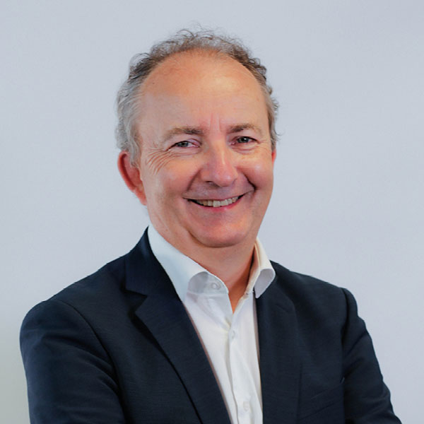
Emmanuel Le Roux
Group EVP, Head of Advanced Computing and AI, Eviden
Bio :
Emmanuel has 30+ years of experience in the IT and telecoms industries successfully developing Worldwide Complex portfolio P&L with a strong Product Management, Business development, Marketing & Sales experiences combined with a deep technical background. Achieved major business growth in different executive positions showing key capabilities to introduce new products and develop product business through strategic partnerships and direct sales go to markets.
Emmanuel is a business and technical expert in Big Data and HPC solutions (HPC infrastructures, Analytics, ML and AI), IT infrastructure (servers, storage, networking), server virtualization, cloud computing, OS, Database, Middleware, OSS/BSS and Voice over IP technologies. Emmanuel developed strong experiences in Global alliances, reseller and OEM contracts with IBM, Hitachi, Dell/EMC, Oracle, RedHat, VMWare and global cloud providers such as Google, Microsoft, AWS, OVH, IONOS…
After being graduated from the High Engineering school in Electronics and Computer Sciences in Rennes (France), Emmanuel held various R&D and Engineering positions in Telecom Wireless division at Nortel in Paris as Software designer, R&D team management and architecture leader.
Emmanuel then moved to different Business senior management roles within Nortel Wireless and CTO global teams, based in Ottawa (Canada) and Paris, overseeing the Nortel Global Management Platform Program, Product Management, Marketing, and finally managing the Global European alliances with IBM.
Emmanuel joined Bull in 2010 as Partner Executive for Oracle, VMware and RedHat, developing the global partnership and new offering combining Bull Product with market leading Software products, managing quick business ramp -up (x3 in joint business) and getting several global partners awards between 2010 and 2013.
In 2014, after the acquisition from Bull by ATOS, Emmanuel was named VP, Head of Enterprise Server, in charge of developing a new server business, leveraging ATOS global market reach combined with the unique Bull High end Computing technologies, ramping up the business up to more than 150M$ in 3 years.
In 2018 Emmanuel was appointed SVP, Big Data Platforms in charge of reformatting the ATOS Big Data Platforms global P&L, combining ATOS Hardware, Software and Expert services to create a unique Edge to Cloud AI Analytics platforms with Business Use case designed for Manufacturing, Public Safety, Retails, Transportation. Emmanuel performed key acquisitions successfully integrated in the ATOS Big Data portfolio, introducing AI, Edge and Complex Analytics capabilities. A new go to market strategy has been implemented through global OEM contract setup with Dell, Cisco and Hitachi, and global provider agreement with Google, Microsoft Azure Thanks to this mixed of technology innovation and extended go to market, the overall business double in 3 years while increasing profitability.
In January 2022, Emmanuel was appointed Group SVP, Advanced Computing, Head of HPC, Quantum and AI. Emmanuel’s role has been extended to HPC, Quantum and AI, managing a worldwide P&L of more than 800M$ per year, with an ambitious plan to grow above 1B$ within 3 years. Emmanuel’s mission is to develop the roadmap and sales strategy to build the first European Exascale machines, develop a broad portfolio of Cloud HPC, Quantum and AI as a Service offering and develop new indirect channel business by signing large OEM and reseller deals to accelerate success in APAC and US markets in complement of the leader position in Europe. Emmanuel’s mission also includes the development of new compute technologies with strategic partners to reinforce the European sovereignty programs for computing and AI.
In May 2024, Emmanuel has been named General Manager for the Big Data and Security division at Eviden, 1.5B€ / year P&L with R&D, factory and product portfolio for Advanced Computing & AI, Cyber Security and Mission Critical Systems.
Abstract :
Stéphane Requena
Director of Technology and Innovation, GENCI
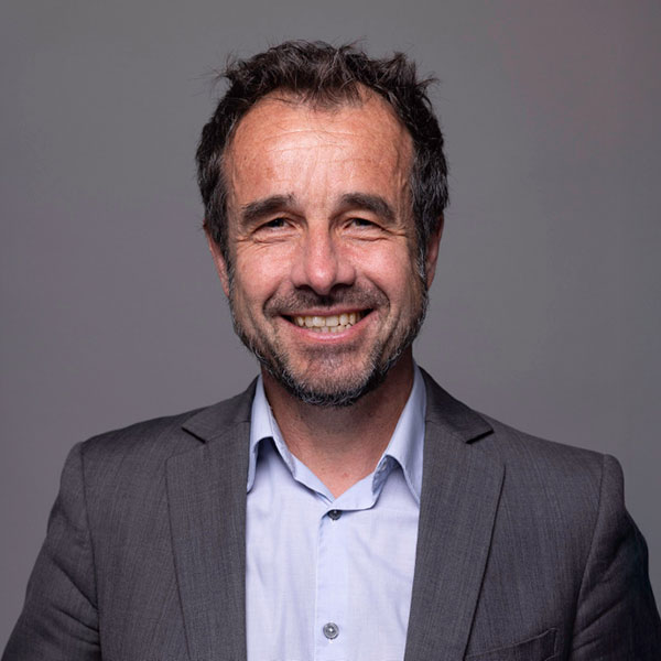
Stéphane Requena
Director of Technology and Innovation, GENCI
Bio :
Stéphane Requena is Director of Technology and Innovation at GENCI (France).
Previously he has been during 10 years in charge of the HPC facilities at Institut Français du Pétrole and involved into optimisation and parallelisation of oil & gas (geology, seismic, reservoir modeling) and automotive applications. He also worked at CS a French service company in parallelising applications in the field of energy for EDF and CEA. At GENCI since 2007 he has been involved in several European projects including PRACE aisbl (as member of the Board of Directors), PRACE implementation projects (Prace-xIP), PPI4HPC (Public Procurement of HPC Innovative Solutions), Mont-Blanc (toward ARM based architectures used for HPC), EPI and EUPEX (toward designing European Processor technologies), EESI (European Exascale Software Initiative) and EXDCI (European eXtreme Data and Computing Initiative) in relation to the scientific and industrial applications roadmaps.
He is also currently involved into EuroHPC as Chair of INFRAG and into the Jules Verne consortium toward the 2nd EuroHPC Exascale system called Alice Recoque.
At GENCI he is also in charge of the development of innovative services related to the use of AI, quantum computing, use of urgent computing for decision making, link with scientific instruments and the technical part of GENCI’s procurements for its HPC, quantum and storage facilities.
Philippe Baptiste
French Minister of Higher Education and Research
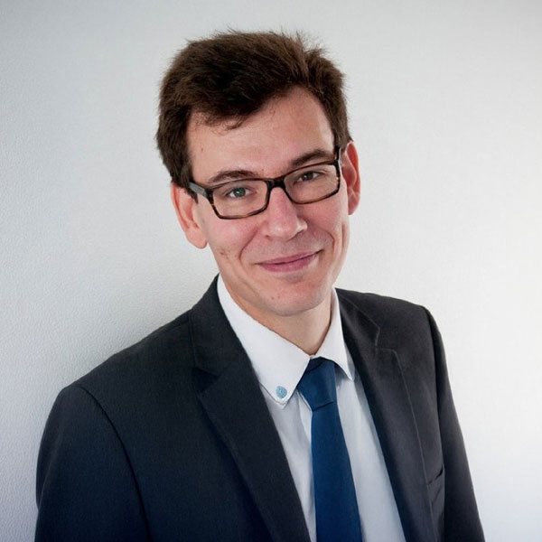
Thomas Skordas
Deputy Director-General, European Commission
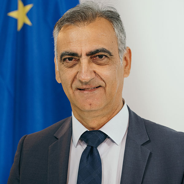
Thomas Skordas
Deputy Director-General, European Commission
Bio:
Thomas Skordas received his Diploma in Electrical Engineering in 1984 and his PhD in Computer Science in 1988. From 1988 to 1995, he worked in France as a Research Fellow and project leader in EU-funded R&D projects in the areas of Information Technology and Robotics.
In 1995, Thomas joined the European Commission as a Research Programme Officer in the Directorate General Information Society & Media (DG INFSO). Since then, Thomas has worked in various units of DG INFSO (which became DG CONNECT in 2012) dealing with ICT research in the context of the EU Research and Innovation Framework Programmes. From 2006 to 2009, he was Deputy Head of Unit for ICT Security and Trust. In 2009, he was appointed Head of the Photonics Unit and in 2014, Head of the Flagships Unit. In March 2017, Thomas was appointed Director of the Directorate for "Digital Excellence and Science Infrastructure” in DG CONNECT and in May 2022, he was appointed Deputy Director-General of DG CONNECT.
Jean-Philippe Fricker
Chief System Architect and Co-Founder, Cerebras Systems
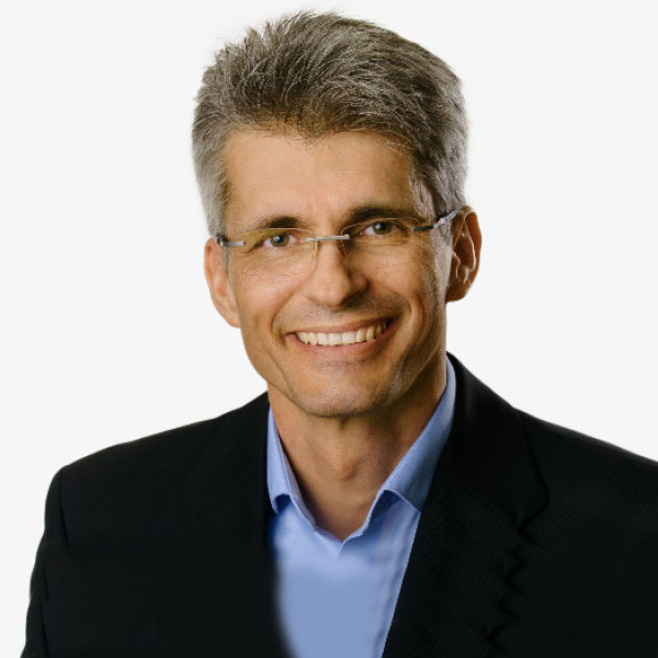
Jean-Philippe Fricker
Chief System Architect and Co-Founder, Cerebras Systems
Bio :
Jean-Philippe (J.P.) is Chief System Architect at Cerebras Systems. Before co-founding Cerebras, J.P. was Senior Hardware Architect at rack-scale flash array startup DSSD (acquired by EMC). Prior to DSSD, J.P. was Lead System Architect at SeaMicro where he designed three generations of fabric-based computer systems. Earlier in his career, J.P. was Director of Hardware Engineering at Alcatel-Lucent and Director of Hardware Engineering at Riverstone Networks. He holds an MS in Electrical Engineering from École Polytechnique Fédérale de Lausanne, Switzerland, and has authored 24 patents.
Louise Frion
Manager new technologies, Institut Montaigne
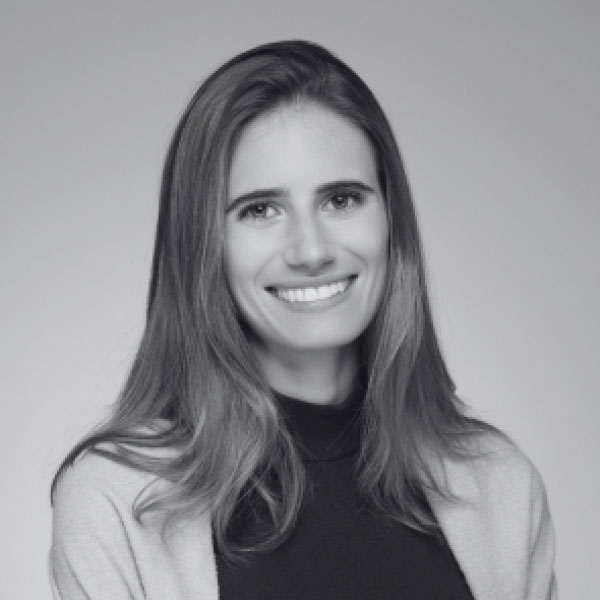
Louise Frion
Manager new technologies, Institut Montaigne
Bio :
Louise Frion is Project Manager - New Technology at Institut Montaigne since February 2024. Louise co-wrote the report Blockchain: consolidating our strengths and the action note Mobilizing and training digital talents published in 2023. Louise previously worked in investment banking at Lazard London in 2017, at the French Treasury in 2018, in the office of the Secretary of State for Digital in 2020 and at Capgemini Invent as a public sector consultant. She also founded Medici&Cie, a consulting and training firm focused on digital strategy for businesses and public administrations.
Louise teaches emerging technologies and their industrial applications in the MBA/EMBA program at HEC Paris. She is a graduate of the Grande École program at EMLyon and holds a Master II in Public Affairs from the École Normale Supérieure and Paris 1 Panthéon Sorbonne.
Philippe Magarshack
MDRF Strategy Office, STMicroelectronics
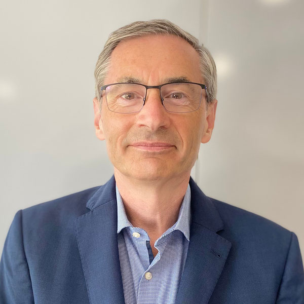
Philippe Magarshack
MDRF Strategy Office, STMicroelectronics
Bio :
From 1985 to 1989, Magarshack worked as a microprocessor designer at AT&T Bell Labs in the USA.
From 1989 to 1994, Philippe was a design manager at Thomson-CSF in France.
In 1994, Magarshack joined ST’s central Technology R&D team in Crolles, France.
From 2005 to 2014, Philippe headed ST’s Design Enablement & Services, and from 2012, focused on growing the 28nm FD-SOI design ecosystem.
In 2015, Philippe became CTO of ST’s Embedded Processing Solutions, where he fostered several strategic customer partnerships.
Since 2016, Magarshack is Group Vice-President in charge of Strategy for ST’s Microcontrollers, Digital ICs and RF Products Group.
From 2014 to 2020, Magarshack was President of the Minalogic Collaborative R&D Cluster in Grenoble France.
Magarshack graduated with Engineering degrees from Ecole Polytechnique, and Ecole Nationale Supérieure des Télécommunications, both in Paris, France
François Andrieu
Head of Memory & Computing Laboratory, CEA-Leti
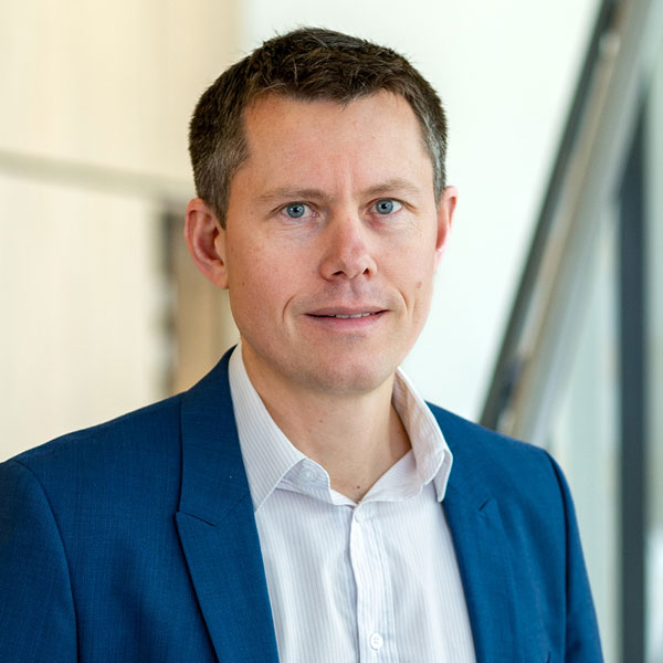
François Andrieu
Head of Memory & Computing Laboratory, CEA-Leti
Dr. François Andrieu is CEA fellow and the head of Laboratory “Nano-devices for Memory and Computing” at CEA-Leti, Grenoble, France.
He has been strongly involved in the development of the Fully-Depleted-Silicon-On-Insulator (FD-SOI) CMOS technology at Leti and with STMicroelectronics, where he was assigned between 2012-2015 in the process-integration and technology-to-design groups. His fields of interest are: NVM Resistive-RAM, In-Memory-Computing, advanced CMOS transistors, 3D-sequential integration.
He is the author or co-author of more than 34 patents, 240 conference abstracts or refereed journal articles, 11 invited papers and 3 book chapters. He received the IEEE senior grade in 2018, the European ERC consolidator grant in 2019 and the IEEE/SEE Brillouin award in 2018.
Michel Paulin
President, French Trusted Digital Solutions Industry
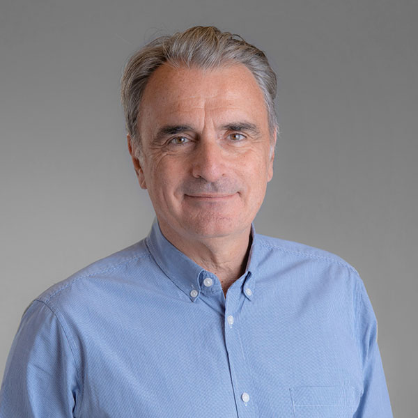
Michel Paulin
President, French Trusted Digital Solutions Industry
Bio:
Michel Paulin spent most of his career in the Tech and Telecom sectors.
He is currently the President « la filière du numérique de confiance » (CSF). An institution which
represents the tech ecosystem players covering software editors, cloud, artificial intelligence,
metaverse, and quantum players).
Three companies have him holding the position of independent Director: one in the quantum field,
one for a datacenter hosting provider, and the last a publisher of B2B billing software.
Previously, during seven years he was the CEO and Director of OVHcloud. During this period,
OVHcloud more than doubled in size, particularly in the US, to become the largest European cloud
provider (over €1 billion in revenue).
An IPO on the Paris stock exchange was completed at the end of 2023.
Previously, he was the CEO of Méditel, and member of the Board Meditel became the secondlargest
telecom operator in Morocco.
He spent 10 years at Neuf Cégétel, where he was CEO and member of the Board This company,
which was listed on the stock market in 2006 before its acquisition by SFR, initially began as a
startup. In 10 years, Neuf Cégétel became France's second-largest fixed-line operator (€3.5 billion
in revenue) through rapid organic growth and also through external growth, acquiring 14 companies
in nine years.
Michel Paulin also spent several years at Groupe Bull, as the VP in charge of the managing network
management and security software BU.
Before that, he participated in numerous assignments in the United States and France at McKinsey
strategy consulting firm and began his career at France Télécom.
Michel Paulin is a graduate of the École Polytechnique and the École Nationale Supérieure des
Télécommunications de Paris, and a member of the Corps des Télécoms.
Miroslaw Klaba
R&D Director, OVHcloud
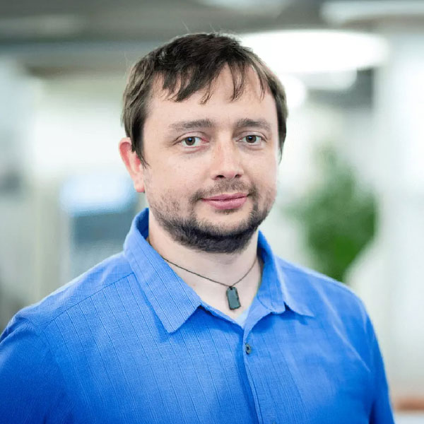
Miroslaw Klaba
R&D Director, OVHcloud
Bio:
Miroslaw is R&D Director of OVHcloud. After earning an engineer degree from ICAM Lille, he joined the OVHcloud family adventure in 2004, holding different positions on project development before taking the position of CIO from 2018. As part of his mission, Miroslaw leads the teams encouraging transformation and participating in the maturity of businesses by providing tools and an information system to help increase effectiveness.
Miroslaw Klaba is member of the Audit Committee.
Miroslaw Klaba is member of the Strategic and ESG Committee.
Hardware at the heart of AI
Elisa Vianello
Edge IA Program Manager, CEA-Leti
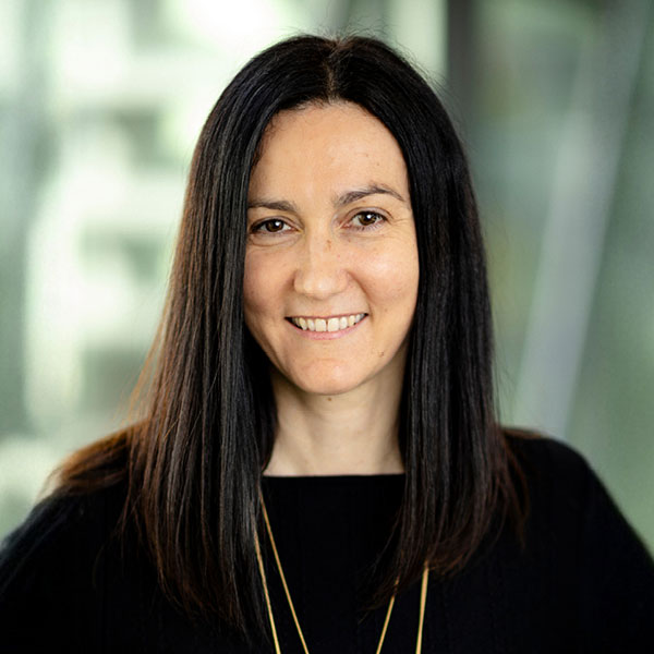
Elisa Vianello
Edge IA Program Manager, CEA-Leti
Bio:
Elisa is a senior scientist at CEA-Leti. She joined the institute in 2011 after spending one year on the research staff at Fondazione Bruno Kessler, Trento. Her current research interests concern the development of new technologies for bio-inspired neuromorphic computing, with special focus on resistive switching memory devices. She has authored or co-authored 4 book chapters and more than 100 technical papers.
She is coordinator of the "MeM-Scales" (2020-2022) European project (H2020) focused on the codevelopment of a novel class of algorithms, devices and circuits that reproduce multi-timescale processing of biological neural systems. In 2022 she won an ERC Consolidator Grant on "Heterogeneous integration of imprecise memory devices to enable learning from a very small volume of noisy data".
She is member of the editorial board of the Neuromorphic Computing and Engineering IOP Science journal (2019-now); associate editor of the Special issue on Emerging Materials in Neuromorphic Computing, AIP APL Material (2020); associate editor of the IEEE Trans. on Circuits and Systems –II (2020-2021).
She received the PhD in Electrical Engineering from the Università degli Studi di Udine (Italy) and the Grenoble Institute of Technology (INPG, France) in 2010.
Dr. Bernd Dielacher
Business Development Manager, EVG
Dr. Bernd Dielacher
Business Development Manager, EVG
Bio
Dr. Bernd Dielacher is business development manager at EV Group (EVG) where he evaluates global market trends and develops growth opportunities for EVG's bonding, lithography and nanoimprint businesses with a particular focus on the heterogenous integration, MEMS, biomedical technology and power device market.
Bernd holds a master’s degree in Microelectronics from Vienna University of Technology and received a PhD in Biomedical Engineering from ETH Zurich.
Abstract:
Heterogeneous Integration and 3D stacking are essential for future system scaling, driven largely by AI. This shift from planar devices to 3D stacked systems relies heavily on bonding technologies. While current devices like image sensors and stacked memory have been specifically designed for 3D integration and bonding, the next phase will trigger new integration processes. Therefore, wafer-level as well as die-level hybrid bonding technologies are being developed, depending on interconnect density, chip size, system yield, and cost. This presentation will cover industry trends and technological advancements in wafer-to-wafer and die-to-wafer hybrid bonding, highlighting key differentiators and integration scenarios, including disruptive device flows with IR laser-based carrier solutions for ultra-thin 3D devices.
Jamie Schaeffer
Vice President - Product Management, Globalfoundries
Jamie Schaeffer
Vice President - Product Management, Globalfoundries
Bio:
Jamie Schaeffer is currently Vice President of Ultra-low Power CMOS Product Management at Globalfoundries. In this role he is responsible for business performance and product roadmap strategy for Globalfoundries' FDX (FD-SOI) and FinFET technologies, including embedded non-volatile memory and advanced packaging.
Abstract:
In this talk we will discuss the semiconductor industry's most pressing AI challenges from the cloud to the edge and GF"s essential chip technology solutions addressing these problems.
Giuseppe Desoli
Company Fellow, Senior Director of Artificial Intelligence & Embedded Architectures, STMicroelectronics
Giuseppe Desoli
Company Fellow, Senior Director of Artificial Intelligence & Embedded Architectures, STMicroelectronics
Bio:
Giuseppe Desoli holds a Master and PhD in Electrical Engineering from the University of Genoa. From 1995 to 2002, he worked at Hewlett-Packard Laboratories, developing VLIW microprocessor architectures, compilers, and tools. In 2002 joined STMicroelectronics as an R&D Director and lead microprocessor architect, pioneering multiprocessor systems for embedded SoCs. Since 2012, he is serving as Company Fellow and Chief Architect for the System Research & Application central R&D group, he is the chairman of the ST scientific committee and coordinator for the ST’s Artificial Intelligence Affinity Team, leading the development of different technologies in the field of HW accelerated AI and In-Memory-computing for advanced deep learning applications. He has co-authored over 70 scientific publications and holds more than 60 patents.
Abstracts:
The rapid growth of AI applications demands efficient and scalable computing solutions. In-memory computing (IMC) has emerged as a promising approach to accelerate edge AI workloads but faces challenges due to device and circuit non-idealities, as well as computing architectures capable of sustaining throughput while still delivering high energy efficiency and low cost. Different device technologies, design approaches, and emerging memories are being explored to address these issues. Near-memory, in-memory, and traditional Von Neumann architectures each offer unique benefits and trade-offs in energy efficiency, compute density, and scalability.
Large language models highlight the potential of heterogeneous 3D stacked technologies and IMC for demanding AI workloads. However, issues like on-device learning, security, and error correction add complexity. As AI algorithms evolve, hybrid approaches remain essential for hardware acceleration. This talk will explore the latest trends in advanced algorithms and STMicroelectronics' journey to integrate edge AI into its products.
Subi Kengeri
Corporate Vice President and GM, Systems to Materials, Applied Materials

Subi Kengeri
Corporate Vice President and GM, Systems to Materials, Applied Materials
Bio:
Subramani (Subi) Kengeri is the Corp. Vice President and GM of Systems to Materials at Applied Materials. He joined the company in 2020 to start the AI Systems Solutions initiative, which evolved into the Systems-to-Materials (STM) group, under his leadership. Prior to Applied Materials, Subi held various technical and executive leadership roles at Globalfoundries and TSMC. He began his career at Texas Instruments as a design engineer and has been granted over 50 U.S. patents. He has given more than 100 invited talks and press interviews.
Abstract:
As AI Systems continue to scale, new challenges arise primarily on Performance/Watt and Total Cost of Ownership (TCO). Innovations driven by System-Technology-Co-optimization (STCO) is needed for next generation AI Systems. This talk covers challenges and opportunities for the Semiconductor eco-system.
Philippe Notton
CEO & Founder, SiPearl
Philippe Notton
CEO & Founder, SiPearl
Bio :
Philippe is the CEO and Founder of SiPearl, the company building European high-performance low-power processors for HPC and AI. His original vision of SiPearl came in 2015 while he was leading a division of 2,400 engineers at STMicroelectronics. In 2017, he joined Atos to help set up the European Processor Initiative (EPI) consortium, which aimed to foster the return of high-performance processor design to Europe. In June 2019, he launched SiPearl as a spin-off of the EPI with the support of the European Union. His first generation processor, named Rhea1, will equip JUPITER, the first European exascale supercomputer.
Philippe is a Supélec engineer (1993) and has an Executive MBA from ESSEC & Mannheim (2008).
Abstract :
Firstly, the US export restrictions on AI chips, then the complex geopolitical and economic context between the US and Europe are signals that should not be ignored. All the more so since, for AI, Europe is repeating the mistakes of the early 2000s, when all the European money invested in European internet start-ups essentially benefited the US via GAFAM! With more than €100 billion investment for France and €200 billion for Europe announced at the AI Summit, it is key for our economy that Europe develops its own AI hardware. But, above all, it is key for Europe's technological sovereignty.
Ivan Miro-Panades
Research Engineer, CEA-List
Ivan Miro-Panades
Research Engineer, CEA-List
Bio :
Ivan MIRO-PANADES received the M.S. degree in telecommunication engineering from the Technical University of Catalonia (UPC), Barcelona, Spain, in 2002, and the M.S. and Ph.D. degrees in computer science from Pierre and Marie Curie University (UPMC), Paris, France, in 2004 and 2008, respectively. He worked at Philips Research, Sureness, France and STMicroelectronics, Crolles, France, before joining CEA, Grenoble, France, in 2008, where he is currently a senior expert research engineer in digital integrated circuits. His main research interests are artificial intelligence, the Internet of Things, low-power architectures, energy-efficient systems, and Fmax/Vmin tracking methodologies.
Abstract :
While the field of AI holds immense promise, the embedded domain faces significant challenges, due to limited computational resources and high energy constraints. Deploying complex AI algorithms at the edge is particularly complex, and the use of high-resolution images and high frame rates, although desirable, exacerbates energy consumption issues. This presentation will explore these challenges and discuss potential solutions to optimize AI implementation in resource-constrained environments. To address these obstacles, we introduce an innovative approach that leverages transfer learning to adapt a versatile feature extractor backbone to a wide range of AI tasks, from classification and image segmentation to object detection. We introduce NeuroCorgi, an ASIC implemented in 22nm technology, capable of delivering continuous HD inference at 30 frames per second with a power consumption of less than 30mW. This cutting-edge innovation has been tested and proven effective in various domains, including agriculture, transportation, home and drones. Experience the future of edge AI with NeuroCorgi, where efficiency meets performance.
Eran Briman
VP Marketing and Business Development, Weebit Nano

Eran Briman
VP Marketing and Business Development, Weebit Nano
Bio :
Eran has over 30 years of semiconductor IP industry experience. At Weebit Nano (ASX:WBT), he serves as VP of Marketing and Business Development, leading the company’s ReRAM commercialization efforts. Prior to joining Weebit in 2020, he was VP of Marketing and Business Development for Corephotonics, an imaging IP start-up acquired by Samsung Electronics in 2019. Before that, Eran was VP of Marketing and Corporate Development for Ceva (NASDAQ: CEVA), where he helped to shape the company as a DSP leader. Over more than a decade at Ceva, he held numerous roles including Chief Architect, where he had overall responsibility for next-generation DSP core R&D. He also held engineering and engineering management roles at DSP Group.
Eran holds a B.Sc. in Electrical Engineering from Tel Aviv University and an MBA from the Kellogg Business School at Northwestern University. He holds several patents and has authored numerous technical publications.
François Andrieu
Head of Memory & Computing Laboratory, CEA-Leti

François Andrieu
Head of Memory & Computing Laboratory, CEA-Leti
Dr. François Andrieu is CEA fellow and the head of Laboratory “Nano-devices for Memory and Computing” at CEA-Leti, Grenoble, France.
He has been strongly involved in the development of the Fully-Depleted-Silicon-On-Insulator (FD-SOI) CMOS technology at Leti and with STMicroelectronics, where he was assigned between 2012-2015 in the process-integration and technology-to-design groups. His fields of interest are: NVM Resistive-RAM, In-Memory-Computing, advanced CMOS transistors, 3D-sequential integration.
He is the author or co-author of more than 34 patents, 240 conference abstracts or refereed journal articles, 11 invited papers and 3 book chapters. He received the IEEE senior grade in 2018, the European ERC consolidator grant in 2019 and the IEEE/SEE Brillouin award in 2018.
Silicon photonics
Eléonore Hardy
Silicon Photonics Partnership Manager, CEA-Leti
Eléonore Hardy
Silicon Photonics Partnership Manager, CEA-Leti
Éléonore Hardy joined CEA-Leti in 2018 as a partnership manager specializing in silicon photonics. She holds a Master’s degree in Engineering and has completed a Master of Science in Management & Innovation. With over 20 years of experience in the optics and photonics industry, Éléonore has held key positions at Philips in the Netherlands and Varioptic, a business unit of Corning, in China.
Throughout her career, Éléonore has demonstrated a proven track record of creating long-term value. She successfully developed laser technologies in France, China, and India for Quantel (now Lumibird) and advanced spectrometer solutions in Europe and Asia for Resolution Spectra Systems (now part of Merck).
Currently, Éléonore is focused on identifying and developing new business opportunities in silicon photonics, with a particular emphasis on high-speed optical interconnects, high-performance computing (HPC), 3D sensing, and advanced computing technologies such as neuromorphic computing and quantum photonics.
Benoit Charbonnier
Research engineer, CEA-Leti
Benoit Charbonnier
Research engineer, CEA-Leti
Bio:
Benoit Charbonnier received his engineering degree in 1994 from Ecole Nationale Supérieure des Télécommunications de Paris and received his Ph.D. degree in 1997 on 40 Gbps soliton transmission from the same institution. In 1997, he joined Nortel Network in Harlow, UK, in the Advanced Communications group where he worked on 80 Gbps long haul transmission and then, in 2001, joined Marconi Communications to develop an Ultra-Long Haul 10 Gb/s based transmission products. In 2004, he joined Orange Labs as a research engineer, focusing on next generation optical access networks and particularly on digital signal processing applied to optical communications. In 2015, he moved to CEA-Leti, Grenoble, leading the photonics program within the French Institute of Technology Nanoelec, developing industrial partnerships to promote silicon photonics technologies. He is now in charge of neuromorphic photonics applications within the silicon photonics lab.
Abstract:
Computing with light is gathering interest recently with prospects of ultra high speed computations hence at very low power consumption per operation. Leti's Silicon Photonics Platform with integrated IIIV, Phase Change Materials and Barium Titanate is well suited to deliver high performance low power circuits for computing as well as inference.
Ashkan Seyedi
Director, Optical Interconnect Products, NVIDIA

Ashkan Seyedi
Director, Optical Interconnect Products, NVIDIA
Bio:
As the Director of Silicon Photonics Products at NVIDIA, Ashkan Seyedi is at the vanguard of merging photonics with cutting-edge computing architectures, particularly in the spheres of generative AI and machine learning. Seyedi's expertise in silicon photonics is pivotal to the advancement of hardware technologies that underpin large language models and AI computations.
Since June 2023, he has spearheaded the integration of multidisciplinary teams to create interconnect solutions for next-generation GPU and CPU products. Prior to this, Seyedi served as a Silicon Photonics Product Architect at NVIDIA, where he played a crucial role in developing interconnect technologies over two years.
Before joining NVIDIA, Seyedi was a Senior Research Scientist at Hewlett Packard Labs, where he led a team in developing a commercial process design kit (PDK) for silicon photonics. His tenure there, spanning nearly seven years, included managing projects funded by various US Government agencies and collaborating with external companies on new products and software tools for electronic design automation.
Seyedi holds a Ph.D. from the University of Southern California, where he conducted groundbreaking research in nanowire photodetectors, solar cells, and LEDs, contributing significantly to the field of photonics. His early career also includes a stint as a Testing Intern at Intel Labs, where he worked on silicon modulators and integrated III-V lasers, achieving milestones in high-speed optical communications.
Abstract:
Sylvie Menezo
Founder and CTO, SCINTIL Photonics

Sylvie Menezo
Founder and CTO, SCINTIL Photonics
Bio :
Sylvie Menezo is CTO of SCINTIL Photonics, which she founded in 2019. SCINTIL focuses on the exploitation of two products fabricated from a proprietary laser-augmented Silicon photonic technology: arrays of multiplexed DWDM lasers used as “External Laser Sources” for co-packaged optics and transceiver circuits. Before, Menezo led the Silicon Photonics Lab and Business Development activities at Leti. She previously developed and led fiber optic technologies at Sercel (France and USA), contributed to the development of pump laser processes at Alcatel. She developped DWDM laser arrays during her PhD (CNET) and polymer-modulators at NZAT (USA) as a Research Scientist. She is in the technical committees of OFC, ECOC.
Abstract:
Manufactured in a high-volume CMOS foundry, our “laser-augmented silicon photonics” delivers best-in-class laser performances. DWDM optical transmissions are made possible for very high-volume uncooled applications. We will present two developed circuits: External Laser Sources for co-packaged optics (DWDM DFB laser arrays with on-chip muxes) and Transceivers (Si modulators, Ge receivers with integrated lasers). We will discuss the benefits of laser integration.
Sébastien Cremer
Silicon Photonics Technology Manager, STMicroelectronics
Sébastien Cremer
Silicon Photonics Technology Manager, STMicroelectronics
Bio :
Sébastien Crémer has been a pivotal figure at STMicroelectronics since he joined the company in 2000. Initially, he played a crucial role in integrating passive devices into BiCMOS and CMOS technologies, a foundational step that enhanced the performance and reliability of ST's semiconductor products.
His work in developing 45- and 32-nm embedded DRAM and RF-SOI technologies further underscored his ability to drive innovation and maintain ST's competitive edge in the industry. These advancements have been instrumental in optimizing memory solutions and improving radio frequency performance, which are essential for modern electronic devices.
He is now in charge of Silicon Photonics technology team.
Sébastien Crémer earned his M. Eng. degree from ESPCI in Paris, an M. Sc from Université Pierre et Marie Curie in Paris, and a Ph.D. from Université Joseph Fourier in Grenoble
Abstract:
In 2025, STMicroelectronics will introduce the new silicon photonics PIC100 Platform for 200Gbps/lane PAM4 (100Gbd) products, representing a leading-edge advancement in the field of optical communications and integrated photonics. Among the improvements, compared to our previous PIC25 platform, are a focus on both optical passive devices, thanks to an innovative stack, and active devices
Anthony Mastroianni
Senior Director 3D IC Solutions Engineering, Siemens EDA (DISW)
Anthony Mastroianni
Senior Director 3D IC Solutions Engineering, Siemens EDA (DISW)
Bio :
Tony Mastroianni has extensive engineering management experience in the global semiconductor industry. In recent years, he has focused significantly on advanced ASIC package design workflow development (2.5/3D). He currently leads development of Advanced Packaging Solutions for Siemens Digital Industries Software. Prior to joining Siemens, he served in IC, Operations and 3DIC engineering leadership positions at Inphi and eSilicon. He earned a bachelor’s degree in electrical engineering from Lehigh University and a master’s degree in electrical engineering at Rutgers University. He is the author of several technical articles and has presented at several industry conferences and has been interviewed in several technical publications. He is an active member in the OCP Chiplet Design Exchange (CDX) working group that is actively driving new and open 3D IC standards and workflows.
Abstract :
3D IC Designs leverage advanced packaging technologies to integrate multiple IC’s, referred to as chiplets into a single package. These designs require a highly integrated and collaborative co-design platform integrating system, IC, package and multi-physics simulation tools and workflows as well as a new set of design enablement kits to support a heterogeneous manufacturing supply chain. In this presentation we explore this new co-design platform and design enablement kits which enable the design planning, implementation, verification, manufacturing and deployment of these new 3D IC designs.
Denis Dutoit
Program Manager, CEA-List
Denis Dutoit
Program Manager, CEA-List
Bio:
Denis Dutoit is senior program manager for advanced computing and digital architectures at CEA-List. He coordinated the European ExaNoDe project that developed a computer node demonstrator combining chiplets, an active interposer, and bare dies in a System-in-Package (SiP). He has also contributed to the architecture of the European Processor Initiative (EPI). His current focus is on architecture pathfinding into chiplet-based designs for computing applications including High Performance Computing, automotive electronics and space components. Before joining CEA, he was a system-on-chip architect at ST Microelectronics and ST Ericsson. He has authored or coauthored more than 20 articles, including invited talks and tutorials at IEEE conferences.
Abstract:
In modern High Performance Computing (HPC) systems, the compute node has evolved into heterogeneous and interconnected processing units with huge amount of memory attached, creating a distributed or disaggregated memory scheme within the node. The AI and data intensive workloads necessitate all these units to share their memory and demand high-bandwidth, low-latency network fabrics to efficiently connect all units.
This presentation will explore solutions from CEA for the integration of chiplet-based architectures with micro-led arrays or silicon photonic interposers (STARAC demonstrator) to achieve low-latency interconnects among processing units.
Sylvie Joly
Partnerships Manager 3D integration & Packaging, CEA-Leti
Sylvie Joly
Partnerships Manager 3D integration & Packaging, CEA-Leti
BIO:
Sylvie Joly is currently working as 3D integration and packaging Partnerships Manager at CEA-Leti. Sylvie received M.Sc. in Microelectronics from ISEP "Institut Supérieur d'Electronique de Paris" in 1989. She completed her education with a Master in Marketing and Innovation at the Grenoble Ecole de Management (GEM) in 2001. Prior to this position, she worked for more than 8 years as display business developer at CEA-Leti. In 2004 as Sr. Marketing Engineer in the CEA's Technology Transfer Department, she built a strong experience in setting up and managing technical marketing surveys. Before joining CEA, she spent 10 years in the industry as an R&D engineer, and 8 years as Sales engineer in several companies including Hewlett Packard and Ericsson.
Abstract:
AI applications with their huge processing demands has led to surging interest in optical circuits. Optics is much faster than electronics, but is also more expensive, harder to use. Co-packaged optics (CPO) puts optical circuits in a package with electronics, saving on cost and space and increasing speed. However, the two technologies still use different materials and overall approaches, making them difficult to mesh. Recent breakthroughs in silicon photonics help bridge the gap, but advanced packaging and 3D heterogeneous integration are critical. This presentation covers multi-die packaging challenges as well as examples from CEA-Leti research of current capabilities.
Karim Hassan
Head of Silicon Photonics Laboratory, CEA-Leti
Karim Hassan
Head of Silicon Photonics Laboratory, CEA-Leti
Bio :
Karim Hassan received the Ph.D. degree in physics from the University of Burgundy, Dijon, France, in 2013 on the development of thermo-optical plasmonic routers for telecom applications, in the framework of the European project FP7-PLATON. Since 2014, he has been with the CEA-Leti (France) as a Research Fellow. He has been involved in both industrial R&D projects and collaborative projects either as a technical contributor, as WP Leader and Project Board member. His research interests include the design, fabrication, and characterization of photonics integrated circuits, hybrid III-V on silicon laser sources, and topological optimization for nanophotonics. He has authored or co-authored more than 100 journal publications, conference papers, and patents. Since 2022, Karim HASSAN is the Head of Silicon Photonics Laboratory under the Optics and Photonics Division at CEA-Leti.
Abstract :
Silicon photonics has established new standards for high-speed interconnects. While the past decade has opened the potential industrial use cases to broader emerging applications, from 3D Sensing to Quantum photonics, the core technologies are permanently challenged to follow the growing computation needs and subsequent communication traffic, mostly driven by generative AI today. A review of the advances of photonic integrated circuits based on SOI and SiN platform will be exposed in order to comment how those two core technologies can answer these challenges by themself and through heterogeneous and 3D integration.
Daniel Pérez López
Founder and CTO, iPRONICS
The keys to sustainable ICs
Laurent Pain
Sustainable Electronics Program Director, CEA-Leti
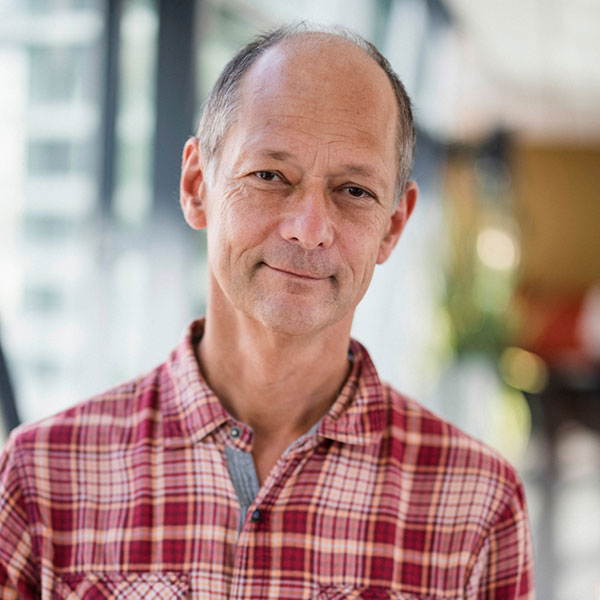
Laurent Pain
Sustainable Electronics Program Director, CEA-Leti
Bio:
Laurent Pain is graduated from the Ecole Nationale Supérieure de Physique de Grenoble in 1992. He received his Ph D after his work on DUV resists study. He joined CEA-Leti in 1996 to work on infra-red technology, and then came back to STmicroelectronics in 1999 working on 193nm and e-beam lithography technologies.
From 2008 to 2014, Laurent Pain leaded the lithography laboratory of the silicon technology division of CEA-Leti. He was also managing in parallel the industrial consortium IMAGINE dedicated to the development of multibeam lithography with MAPPER lithography BV.
Since July 2014, within the CEA-Leti Silicon Technology Division, he is now in charge of the business and the partnerships developments of the Silicon Technologies Platform Division.
Abstract:
The semiconductor industry underpins global digital transformation, with the ICT market expected to double by 2030 due to advances in AI, 5G, and cloud computing. A fundamental shift toward more resilient, sustainable, and circular manufacturing models is required to enable this growth. Key challenges include reducing water, gas, and metal consumption, minimizing PFAS dependence, and improving effluent circularity.
Attendees will hear how CEA-Leti’s comprehensive sustainability roadmap spanning the entire semiconductor value chain will integrate process innovation with system-level optimization to drive measurable environmental impact reduction. The SubFAB Labs initiative, developed in collaboration with International SubFAB Research Labs (ISRL), is a central pillar of the roadmap. This four-year program, which can be extended, will evaluate the subfab environment, from process to final waste treatment by improving material use, abatement strategy and global effluent? circularity. The aim is to reduce costs and global environmental impact.
Jessica DeMott
R&D Manager for Fluorospecialities, Arkema
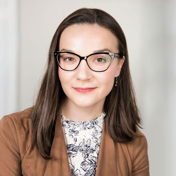
Jessica DeMott
R&D Manager for Fluorospecialities, Arkema
Bio:
Jessica DeMott is an R&D Manager for Fluorospecialities at Arkema with a focus on new molecule and new application development including the development of next generation, low global warming potential and partially fluorinated precursors for etch applications. She received her PhD in organometallic chemistry from Texas A&M University in 2015 then worked for BASF before joining Arkema in 2019. She is based out of Arkema’s North American Headquarters in King of Prussia, PA.
Abstract:
The identification and development of next generation, low global warming potential (GWP) etch precursors includes access to novel chemistry. Arkema’s research is focused on establishing and optimizing manufacturing routes to new etch molecules. Considerations for providing a sustainable supply chain for new fluorinated etch gases will be discussed.
Cathy Batisson
Lead of European Partnerships and Public Funding, Renault Group
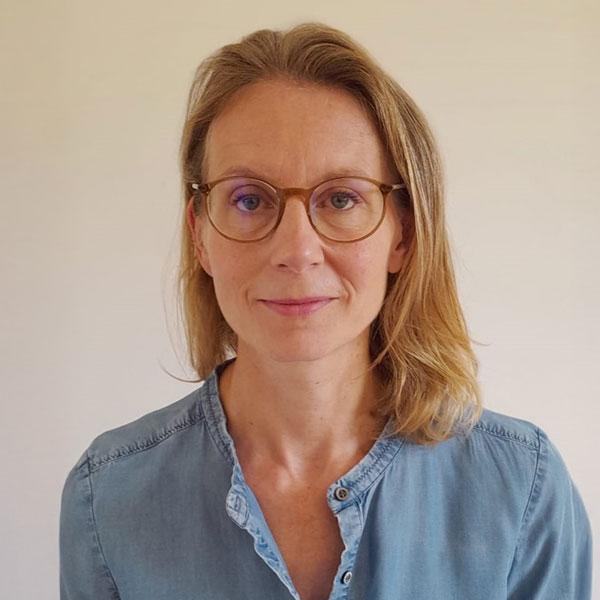
Cathy Batisson
Lead of European Partnerships and Public Funding, Renault Group
Bio:
Cathy Batisson holds an engineering degree in Energy Engineering from the Institut National des Sciences Appliquées of Lyon and a Powertrain Engineering degree from the IFP School. She began her career at Renault in 1998 as a software developer, working on an innovative near-zero emission gasoline vehicle. Over the years, she has held various management positions in powertrain innovation, focusing on control, sensing, and calibration. Since 2011, she has served as the Gasoline Engine Innovation Program Manager.
Since 2021, she has been leading the European Research and Innovation Partnerships and Public Funding, managing European collaborative projects for the Group. Additionally, she is responsible of the IPCEI ME/CT project for Renault and acts as Deputy Work Stream Leader for the Work Stream ACT (power and actuation).
Abstract:
A holistic approach:
- 3 pillars: carbon neutrality, conserve resources, preserve biodiversity
- Life-cycle assessment, “cradle-to-cradle”
Stakes & solutions along the value circle
- “Reduce consumption” - Production & Supply
- “Extend the lifespan of vehicles and parts” - Usage
- Recycle
Some Examples at Renault Group with Embleme concept car & The Future Is Neutral
Axelle Weber
Data Scientist, Schneider Electric
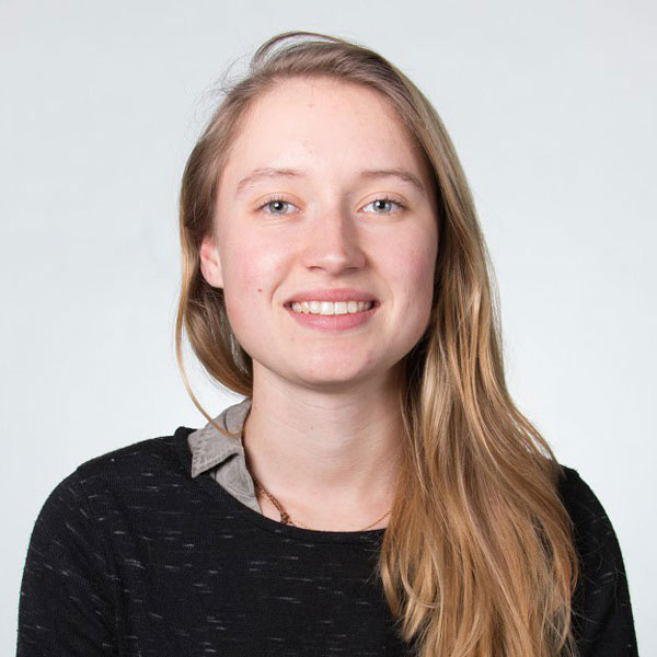
Axelle Weber
Data Scientist, Schneider Electric
Bio:
Graduated from Bordeaux INP in 2019, I joined Schneider Electric as a data scientist in 2022. I have interests in applied artificial intelligence, especially in the fields of energy, agriculture, and medicine, as well as sustainability topics. At Schneider Electric, I've been involved in projects that assess the environmental impact of digital solutions.
Abstract:
At Schneider Electric we place sustainability at the core of our principles. Thus, an important part of our activities focuses on energy management in buildings. This is where microgrids have a crucial role to play.A microgrid is a self-contained electrical network that allows you to generate your own electricity on-site and use it when you need it most. It can be applied to any buidling with renewable energy sources such as houses, school or datacenters for example.We use AI for the energy management in microgrids.
In this talk we show the net carbon impact of an AI-based microgrid management solution. It is obtained via a lifecycle assessment, including savings generated by the AI solution, and the carbon footprint of software, including AI, and of hardware (solar panels, batteries).
Nick Duinslaeger
CEO / Co-founder, GRAPHEC
Nick Duinslaeger
CEO / Co-founder, GRAPHEC
Bio:
Nick Duinslaeger is a scientist and entrepreneur focused on innovative water treatment solutions. He holds an MSc in Catalytic Science and Technology from the Catholic University of Leuven and began his career as a project manager at Veolia Water Technologies, designing wastewater treatment plants in the Benelux region. He later worked with Médecins Sans Frontières as a Technical Referent in Environmental Health. Nick completed a PhD on novel anode materials and nano-electrochemical systems for PFAS degradation in wastewater. He is the co-founder and CEO of GRAPHEC, a company pioneering graphene-enabled electrochemical processes to remove PFAS, combining cutting-edge technology with a strong commitment to environmental sustainability.
Abstract:
The persistence of PFAS in semiconductor wastewater presents critical environmental and regulatory challenges. This presentation compares emerging PFAS degradation technologies, analyzing their strengths and limitations in terms of scalability, energy efficiency, and integration potential within existing treatment systems. By addressing key pain points, we will explore the most viable pathways for the semiconductor industry to adopt sustainable and effective PFAS removal solutions.
Jacques Kluska
Principal, Responsible AI Specialist, Schneider Electric
Jacques Kluska
Principal, Responsible AI Specialist, Schneider Electric
Bio:
Jacques is an engineer who graduated from Ecole Nationale Supérieure des Arts et Métiers in 2010 and got a PhD in astrophysics from CNRS/Grenoble-Alpes University in 2014. He has extensive experience in developing generative AI models for astrophysical imaging during his time as an associate researcher at the University of Exeter, UK, and KU Leuven, Belgium. Joining Schneider Electric's AI hub in 2023, Jacques worked in diverse AI use cases such as predictive maintenance, time series, and computer vision. He is now leading the Sustainable AI pillar within the Responsible AI team. Jacques has been actively involved in shaping the development of the AFNOR spec on Frugal AI, the first global reference on the topic published in June 2024.
Abstract:
At Schneider Electric we place sustainability at the core of our principles. Thus, an important part of our activities focuses on energy management in buildings. This is where microgrids have a crucial role to play.A microgrid is a self-contained electrical network that allows you to generate your own electricity on-site and use it when you need it most. It can be applied to any buidling with renewable energy sources such as houses, school or datacenters for example.We use AI for the energy management in microgrids.
In this talk we show the net carbon impact of an AI-based microgrid management solution. It is obtained via a lifecycle assessment, including savings generated by the AI solution, and the carbon footprint of software, including AI, and of hardware (solar panels, batteries).
Philippe Garnier
Senior Member of Technical Staff – Wet & Bonding R&D, STMicroelectronics
Philippe Garnier
Senior Member of Technical Staff – Wet & Bonding R&D, STMicroelectronics
Bio :
With 25 years of experience in wet process technology for semiconductor manufacturing, Philippe is an R&D senior expert in materials and surface preparation at STMicroelectronics.
He has developed pioneering wet single wafer tools and gate oxide patterning techniques. His innovations have improved manufacturing efficiency, reduced costs, and enhanced product quality. In addition, Philippe supervises PhD studies on topics such as wetting, acoustics, wet chemistry infiltration, and particle removal.
Senior Member of the ST Technical Staff, Philippe has an MS in Chemistry from ENSIACET, Toulouse. He has published over 60 papers at international conferences.
Abstract:
The semiconductor industry encounters substantial challenges in developing new chemical formulations, including stringent quality control, environmental safety and health concerns, performance optimization, and cost management. This presentation delves into these challenges across the entire life cycle of chemical formulations, from initial availability and ease of use to end-of-life recycling. It underscores the critical need for a collaborative approach involving chemical suppliers, semiconductor manufacturers, and demo labs (R&D labs or tool suppliers) to effectively address these requirements and drive innovation in semiconductor manufacturing.
Marie Bouvet
Critical Materials & Minerals Analyst, OFREMI / BRGM
Marie Bouvet
Critical Materials & Minerals Analyst, OFREMI / BRGM
Bio :
Marie Bouvet dit Marechal is Critical Minerals & Materials Analyst at OFREMI (French Observatory of Mineral Resources for Industrial Sectors) / BRGM (French Geological Survey).She has especially been involved in setting up and coordinating OFREMI’s working group on Stress-Test (gallium, germanium, graphite, tungsten...), which intends to assess the risks and impacts of critical minerals supply disruptions on the industrial sectors in the perspective of strenghtening the french and european sovereignty. She contributes with OFREMI's team to support the European Commission in implementing the Critical Raw Materials Act in this matter.
Abstract :
Mathilde Billaud
Research engineer, CEA-Leti

Mathilde Billaud
Research engineer, CEA-Leti
Bio :
Mathilde Billaud is a researcher in the eco-innovation program of CEA-Leti since December 2023. She investigates interconnection technologies and non-volatile memories. She carries out life cycle analysis of microelectronic components to promote more sustainable solutions. She also investigates repairability options in interconnection technologies. Between 2013 and 2017, she was part of the Environmental Engineering Department at Fraunhofer IZM in Berlin. She holds a PhD in microelectronics from the University of Grenoble Alpes, France.
Abstract:
The situation is alarming: the worldwide generation of electronic waste is rising year on year and the demand for higher performance is driving hardware renewal more frequently. We will present CEA-Leti's strategy for improving the longevity of semiconductors through reliability, reuse and repair.
Jérôme Boutet
Senior Data Scientist, CEA-Leti

Jérôme Boutet
Senior Data Scientist, CEA-Leti
Bio :
Jérôme Boutet graduated from the Ecole Nationale Supérieure de Physique de Grenoble in 2000 and became also a Doctor of the Université Grenoble Alpes (UGA), France. Soon after, he joined French Atomic Energy Commission (CEA) as a full-time researcher. Now he is a scientific expert in the field of Data Science, Signal processing and Machine Learning. In parallel, he has also been involved in several industry related activities.
Abstract:
Traditional predictive maintenance methods of power converters face trade-offs between accuracy and complexity. This work explores Physics-Informed Machine Learning (PIML) to enhance reliability by combining physical models with neural networks. Case studies include DC-link capacitor monitoring via voltage discharge, improved RUL prediction for MOSFETs, and ultrasound-based diagnostics. PIML improves accuracy, reduces data needs, and ensures physically consistent outputs, offering a promising path for advanced, non-invasive condition monitoring.
Stéphanie Cottin
Sustainability & Safety Director, Soitec

Boubakr Rahmani
Research Engineer, CEA-Leti
Boubakr Rahmani
Research Engineer, CEA-Leti
Bio :
Dr. Boubakr Rahmani is a research engineer at CEA-Leti in Grenoble, France, and an alumnus of the Université Grenoble Alpes, where he completed his Ph.D. at the G2Elab (Laboratoire de Génie Électrique de Grenoble). His expertise lies in power electronics, with a focus on sustainability, reliability, and eco-design. Dr. Rahmani's research encompasses the development of methodologies for monitoring the residual value of power electronic components, aiming to enhance their reuse and reliability. He has contributed to the field through publications on topics such as predictive lifetime monitoring and the integration of circular economy principles into power electronics design.
Abtsract:
In the context of increasing demand for secure and sustainable smartphone reuse, this work explores the use of X-ray irradiation as a method for total data erasure from flash memory. The objective is to enable safe reuse or recycling of devices without compromising data confidentiality. We present experimental results on the impact of X-rays on memory retention and physical degradation, and evaluate the feasibility of this method as a non-reversible, low-invasiveness solution for secure data destruction in circular electronics.
Yannick Rivoira
Sustainability Engineer, CEA-Leti
Yannick Rivoira
Sustainability Engineer, CEA-Leti
Bio:
Yannick Rivoira is a sustainability engineer at CEA-Leti since 2022. He is especially involved in environmental impacts assessments for microelectronics industry. This imply methodological development, data collection and comprehension at process and fab level as well as understanding the environmental issues and reglementations. He is specifically in charge of the Sustainability work package for the european project FAMES.
Abstract:
Microelectronics is a high-precision industry that is rapidly evolving. Better understanding its environmental implications and making this industry more sustainable is a complex challenge. This is why, inside the FAMES european project, a methodology and a software for assessing environmental impacts are being developed. The main objective is to add an Environmental criterion to the traditional Power-Performance-Area-Cost (PPAC) optimisation by taking into account environmental impacts from design to chip manufacturing.
Aurélien Sarrazin
Research Engineer, CEA-Leti
Aurélien Sarrazin
Research Engineer, CEA-Leti
Bio :
Aurélien Sarrazin is a plasma etching research engineer at CEA-Leti since 2019. He holds a PhD in material sciences from University of Nantes after a 3-year experience at CEA-Leti on "Development of advanced techniques for patterning sub-10 nm CMOS processes". In 2023, he worked with a trainee engineer on a Life Cycle Assessment of plasma etching processes. Since 2024, he also coordinates sustainable actions for the patterning department. In the 3 following years, he will be involved in GENESIS program, a EU flagship project on sustainability in microelectronics.
Abstract:
The growth of semiconductor market and its environmental footprint impose to rethink its value chain. GENESIS, a EU flagship program, has been launched on this topic in May 2025 with 58 partners and the CEA-Leti is the project coordinator. This project aims to improve less impacting material development, process tailoring, air emissions sensing and waste reduction monitoring. For example, development of PFAS-free resists and evaluation of low GWP gases will be performed in order to reach more sustainable patterning processes. Interests of these alternative materials will be evaluated for the whole value chain (morphology, emission, wastes, etc.).
Virginie Delay
CSR & conformity Director, SGH Medical Pharma
Virginie Delay
CSR & conformity Director, SGH Medical Pharma
Bio :
As a medical plastics and devices specialist, I have been working on ESG issues for over five years. Working for a company that manufactures single-use polymer medical devices, I strive to understand, analyse and reflect on different ways of doing things, changing business models to make the company more resilient, using LCAs and product carbon footprints, for example, to reduce our environmental impact as much as possible. I am active in several ecosystems and work daily towards reducing our sector's emissions.
Abstract:
Due to the regulatory constraints applicable to medical devices and stakeholders' desire to improve the circularity of these devices and reduce their negative impact, manufacturers in the medical device industry are turning to eco-design, which is one of the most effective ways of addressing this issue. Reusing DM raises many questions, and while it is applicable to some, it cannot be generalized.
Cécile Vaugelade
Regulatory Affairs Director, Snitem
Cécile Vaugelade
Regulatory Affairs Director, Snitem
Bio :
Cécile Vaugelade, a chemical engineer by training, began her career at the french sanitay agency in the field of medical device reimbursement and then in medical device market surveillance (market control, vigilance, regulatory affairs, clinical trial authorization, etc.). She then worked at LNE/G-MED, a French notified body, as head of the G-MED certification center for over three years before joining SNITEM as Director of Regulatory Affairs in 2018.
At SNITEM, she is responsible for managing regulatory activities covering a wide range of topics (CE marking, advertising, clinical investigations and evaluations, health vigilance, environmental regulations, end of life of medical devices, standardization, etc.).
Abstract:
Due to the regulatory constraints applicable to medical devices and stakeholders' desire to improve the circularity of these devices and reduce their negative impact, manufacturers in the medical device industry are turning to eco-design, which is one of the most effective ways of addressing this issue. Reusing DM raises many questions, and while it is applicable to some, it cannot be generalized.
Mélanie Alias
Sustainable Advisor for Healthcare technologies, CEA-Leti
Mélanie Alias
Sustainable Advisor for Healthcare technologies, CEA-Leti
Bio :
Researcher at the CEA since 2011. After 10-year career in energy storage : (PhD on negative electrode materials for Li-ion batteries (2008), and missions around battery monitoring by sensors (reference electrodes, acoustics), I moved into another field, healthcare, by developing electrochemical sensors. Since 2022, I have accepted a new role: advisor for more sustainable innovation (awareness-raising, support, eco-design).
Abstract:
The CEA Technological Research Division’ team is designing innovative microfluidic circuits for allergen detection in food. Beside this technological development, one of our main concerns is related to the eco-innovation issues (materials, manufacturing processes, energy and water consumption, …) regarding such embedded labs. As an illustration, we propose hereby to describe the environmental footprint of an actual microfluidic card and to draw forward eco-design-proposals to reduce its ecological impact, including its future industrial context of use.
Klaus Kuemmerle
Director Global Sales, Pfeiffer Vacuum & Fab Solutions
Klaus Kuemmerle
Director Global Sales, Pfeiffer Vacuum & Fab Solutions
Bio :
Klaus Kuemmerle is Director Global Sales for the abatement business at Pfeiffer Vacuum + Fab Solutions.
He has over 25 years international experience in the high-tech semiconductor industry.
Klaus specializes in abatement technology and cleanroom contamination control. His focus is on sustainable solutions that reduce emissions and energy use in subfabs.
Klaus has held leadership roles in global sales, project management and business development.
Klaus holds a Degree in Physics Engineering (Dipl. Ing. FH) from the University of Applied Sciences Heilbronn/Germany and is certified EUREM Energy Manager.
Abstract:
This presentation introduces the Busch Group including Pfeiffer Vacuum + Fab Solutions and its commitment to sustainable semiconductor manufacturing.
It highlights semiconductor industry challenges in reducing greenhouse gas emissions and outlines innovative subfab solutions.
Key focus areas include SMART abatements, Hydrogen recycling and intelligent emission control.
Slava Libman
CEO, FTD Solutions
Slava Libman
CEO, FTD Solutions
Bio:
Dr. Slava Libman is a thought leader, passionately driving innovation in sustainability with over 25 years of experience in water technology. As a Co-Founder and CEO of FTD Solutions, he leads an early-stage company dedicated to helping complex industrial facilities tackle sustainability challenges through the use of advanced digital twins. These tools empower organizations to visualize their data, diagnose issues, and make data-driven decisions to optimize performance.
Under Dr. Libman's leadership, FTD Solutions has assembled a highly skilled team that has collaborated with numerous global corporations to solve countless challenges. Their combined efforts have resulted in savings of hundreds of millions of dollars, risk mitigation, and an impressive water conservation record reaching billions of gallons. Slava's unwavering commitment to sustainable practices and technological advancements positions him as a thought leader in the industry.
Slava champions environmental and operational sustainability in the semiconductors via industry wide activities. He is a co-chair of Environmental Sustainability forum of IRDS, Yield Enhancement forum of IRDS, as well as SEMI Standards Water Reuse Task Force. Slava is a lead moderator of the International UPM Conference driving innovation in semiconductor facilities.
Morten Eikenes
CCO & CTO, LayerOne AS
Morten Eikenes
CCO & CTO, LayerOne AS
Bio:
Dr. Morten Eikenes is a commercial executive with a PhD in organic chemistry with over 20 years of experience in advanced materials, nanotechnology, and sustainable chemistry. As CCO at LayerOne AS, he leads global commercialization of graphene materials. He has held leadership roles at Jotun, Nopco, Solenis, and Bioenvision, where he transformed R&D innovations into market-ready solutions. Known for bridging science and strategy, Dr. Eikenes contribute with scaling deep-tech, product-market fit, and innovation in industrial sectors.
Power and radiofrequency
Philippe Despesse
Deputy Director of Programs, Systems Division, CEA-Leti
Martin Gallezot
Deputy Head Silicon Components Division, CEA-Leti
Martin Gallezot
Deputy Head Silicon Components Division, CEA-Leti
Bio:
Martin Gallezot graduated from Ecole Supérieure d’Electricité, Paris, France in 1993 with a Msc in Electrical Engineering. He is responsible for technology transfer in the Silicon Components Division at CEA-LETI. Before that he held several technical and business positions in semiconductor IP companies operating in the cybersecurity, high speed interconnect and flat panel display industries.
Swan Gerome
RF & Telecommunications Industrial Partnership Manager, CEA-Leti
Swan Gerome
RF & Telecommunications Industrial Partnership Manager, CEA-Leti
Bio:
Swan GEROME is Technology Partnership Manager within the Systems Department, with a focus on RF and Telecommunications at CEA-Leti.
He holds a degree in Marketing and Sales Management from Grenoble IAE and has over 15 years of experience in the semiconductor industry across materials, design, and research companies.
From 2008 to 2014, he served as Sales Manager at Dolphin Integration, developing business for ASIC design, analog silicon IP, and libraries for foundries, fabless companies, design houses, and OEMs. He also managed a team of sales coordinators in Asia (Japan, South Korea, and Taiwan) as well as in Europe.
He joined CEA-Leti in 2015 as Industrial Partnership Manager for the Systems Department, covering sensor integration, energy management, embedded data processing, and RF telecommunications (antenna design and integration, protocols development, and RFIC design). In this role, he developed partnerships with national and international companies, ranging from startups to Big Tech.
Between 2022 and 2023, he was Product Marketing Manager for the Connect-SOI Business Unit at Soitec, where he developed the roadmap for engineered silicon substrates for RF applications and launched new products to address market requirements.
Abstract:
Harnessing dielectric permittivity the property that describes how electric fields propagate through matter CEA‑Leti researchers have built a non‑invasive, chip‑scale technology that maps the hidden electrical signatures of cells and materials.
The device emits radio‑frequency from 30KHz to 30GHz, captures transmitted and reflected signals, and decodes them with a silicon‑integrated vector network analyzer (VNA). This yields an ultra‑miniaturized, low‑cost, low‑power, wide‑band system that can be embedded in portable and wearable devices.
This session will show how CEA-Leti enables non-invasive detection across multiple sectors, such as health care, wellness, agri-food, and automotive by converting dielectric permittivity maps into actionable insights. The technology unlocks a world of applications ranging from cancerous-cell detection, hydration monitoring, process monitoring, and proximity detection.
Sylvain Bacquet
Head of Power Electronics and Energy Management lab, CEA-Leti
Michel Bommer
UPS Technology Director, Legrand

Michel Bommer
UPS Technology Director, Legrand
Bio:
Michel held various leadership roles for new technology introduction in the UPS industry.
He started his career in 1985 in SOCOMEC a French company specialized in UPS solutions as R&D engineer. Later in 1999, he reached the position of R&D Director in the UPS Division.
In 2011 , he joined the LEGRAND Group as R&D Director for the new UPS Division just created.
Currently ,he is in charge of technology as Director for the UPS R&D department of LEGRAND. He is also IEC expert in the SC22H related to UPS standardization.
He has 40 years of experience in UPS design , and application such as Data Center segment.
Michel is a graduate of INSA Lyon in Electrical Engineering.
Abstract:
Stéphanie Robinet
Head of Analog and Mixed-IC Design Lab, CEA-Leti

Stéphanie Robinet
Head of Analog and Mixed-IC Design Lab, CEA-Leti
Bio:
Stéphanie Robinet is the Head of analog and mixed-signal Integrated Circuits Lab in Silicon Components Department in CEA-Leti. After master’s degree graduation from Institut Polytechnique de Grenoble (now University Grenoble Alpes) in 1999, she has been mainly involved in research projects for low power sensors and implantable applications, among them BCI Wimagine implant as ASIC design leader. Since 2013, she has led a research design team in three different Leti divisions, experiencing intimately the system to technology links and benefits of co-design. She is targeting innovation in integrated systems, merging advanced mixed-signal integrated design and new silicon components capabilities for many applications domains.
Abstract:
With the increasing demand for computing resources and the rapid expansion of AI-based applications, traditional computing system architectures are reaching their limits. For many years, systems have been designed with a primary focus on data and bandwidth constraints, but their performance is now being hindered by power efficiency and the distribution of high currents within the systems. The development of highly efficient point-of-load converters capable of vertically distributing power in high-performance computing systems is bringing together the power, IC design, and integrated silicon communities to find common solutions.
Yann Lamy
Head of Power Devices Lab, CEA-Leti
Yann Lamy
Head of Power Devices Lab, CEA-Leti
Bio:
Yann Lamy is the head of the Power Devices Laboratory which is leading advanced R&D on Wide Band Gap (GaN and SiC) and ultra WBG (Diamond) semiconductors, through academic and industrial projects at CEA LETI. Previously, he has managed a large scale program on engineered wafers, enabling in particular the performance of power semiconductors. Yann LAMY was the R&D Lab Manager for RF and passive components, successfully transferring R&D results to industry.
He holds a PhD in Material Engineering and Hyperfrequency, a Master degree from ESPCI Paris and has authored or co-authored over 50 peer-reviewed publications.
Abstract:
Wide Bandgap (WBG) materials, such as Gallium Nitride (GaN) and Silicon Carbide (SiC), are increasingly crucial for powering datacenters due to their superior efficiency and reduced energy losses. These materials enable higher power densities and improved cooling, leading to significant cost savings and reduced environmental impact. As datacenter power demands grow, particularly for AI applications, WBG materials offer a sustainable and efficient solution for meeting future energy needs.
Francesco Foglia Manzillo
Research Scientist in Applied Electromagnetics, CEA-Leti
Francesco Foglia Manzillo
Research Scientist in Applied Electromagnetics, CEA-Leti
Bio :
Francesco Foglia Manzillo received his M.Sc. in Electronics Engineering from the University of Naples "Federico II" in 2012, and his Ph.D. from the University of Rennes 1, France, in 2017. He held research positions at Delft University of Technology, NXP Semiconductors, and the University of Michigan during his studies.
Since 2017, he has been an Antenna Scientist at CEA-Leti in Grenoble, focusing on antenna arrays, electromagnetic surfaces, millimeter-wave integration, and beamforming systems.
He has co-authored over 80 publications, holds 7 patents, and has contributed to more than 16 national and European R&D projects.
His work has been recognized with the Best Applied Technology Antenna Paper Award at EuCAP 2024, the Young Engineer Prize at EuMC 2021, the Best Innovation Award at the ESA Antenna Workshop in 2018.
Abstract :
Rethinking the design of wireless systems through holistic approaches is crucial for achieving true energy efficiency without compromising performance. This talk introduces innovative architectural solutions and system-level methodologies for the co-design of radiofrequency (RF) front-ends and antennas. Case studies, ranging from antenna-transceiver impedance co-optimization in phased arrays to low-power, broadband beamforming with flat lens antenna systems at millimeter waves, will demonstrate the advantages of this paradigm over conventional decoupled approaches.
Additionally, a perspective on three-dimensional (3-D) advanced packaging solutions for tightly integrating circuits and antennas within low-loss multilayer modules will be presented. These system-level and technological innovations pave the way toward the next generation of multifunctional, sustainable and scalable wireless communication systems.
Thierry Bouchet
CEO & Co-Founder, Wise Integration
Thierry Bouchet
CEO & Co-Founder, Wise Integration
Bio:
Thierry Bouchet holds a PhD in Electrical Engineering (2001). He began his career in the semiconductor industry, working at IBS (Ion Beam Services) and Atmel, where he developed strong expertise in advanced semiconductor manufacturing technologies and electronic components.
In 2011, Thierry founded his first fabless startup, ADIS, specializing in power electronics for niche markets.
He then joined CEA LETI as Strategic Marketing Manager for energy and power electronics. This role enhanced his industrial insight and deepened his understanding of miniaturization challenges, energy efficiency, and strategic market positioning.
Building on this experience, Thierry launched on 2020 Wise Integration, an innovative startup that delivers the ultimate power supply miniaturization solution using GaN-based integrated circuits and digital control. He successfully led the company through two funding rounds.
Abstract:
In a world increasingly driven by electrification and efficiency, Wide Bandgap (WBG) semiconductors—such as GaN and SiC—are redefining the boundaries of power conversion. Yet, unlocking their full potential requires more than just faster switching and lower losses. It demands a system-level approach, where digital control becomes the key enabler of performance, intelligence, and adaptability.
This presentation explores how high-performance digital control architectures, when co-designed with WBG-based power stages, elevate system-level capabilities across efficiency, dynamic response, and reliability.
The audience will gain insights into how digital control acts as the “software brain” of modern power conversion systems ready for tomorrow’s applications.
Emilio Calvanese Strinati
Smart Devices, Telecommunications & Security Strategy Program Director International Research Programs, CEA-Leti
Emilio Calvanese Strinati
Smart Devices, Telecommunications & Security Strategy Program Director International Research Programs, CEA-Leti
Bio :
Abstract :
Guillaume Vivier
Senior Manager, Standardization & Strategy, Qorvo
Guillaume Vivier
Senior Manager, Standardization & Strategy, Qorvo
Bio :
Guillaume Vivier received the M.Sc. degree in telecommunication engineering from Télécom Paris, Paris, France in 1993 and the Ph.D. degree from the University of Pierre and Marie Curie, Paris. After various positions with Alcatel and Motorola, he joined Sequans Communications to drive innovation into products. As CTO and head of CTO office, he coordinated standardization and system architecture activities, advanced R&D and partnerships and he initiated 5G activity. In 2022 he joined Qorvo to develop UWB standardization. He is currently involved in various wireless connectivity standard organizations.
Abstract:
Ultra-wideband communication has been introduced more than 20 years ago. More recently, this technology had a significant traction for its ranging capability and was introduced in consumer devices. This presentation focus on sensing capability of UWB, introducing the technical concepts and discussing the possible applications.
Christophe Villien
Research Engineer, CEA-Leti
Christophe Villien
Research Engineer, CEA-Leti
Bio :
Christophe Villien, Eng., PhD, joined CEA-LETI in 2006. His expertise lies primarily in Bayesian fusion algorithms applied to a wide range of sensors, including IMUs, magnetometers, and odometers, as well as radio technologies such as UWB, LoRa, and 5G signals. He has contributed to and managed numerous industrial and institutional projects.
Abstract :
In places where GPS doesn’t work well, drones often rely on UWB signals for positioning and radar to avoid obstacles. We introduce a new method that turns low-cost UWB devices into simple radars, removing the need for extra equipment. Despite the challenges of using this from a moving drone, our approach accurately detects obstacles and improves positioning. Field tests showed up to 50% better accuracy compared to UWB alone
Marc Maranzana
Head of Digital Technologies, COLAS
Marc Maranzana
Head of Digital Technologies, COLAS
Bio :
Marc Maranzana is a seasoned expert in innovation, digital transformation, and
investment strategy, with over 25 years of experience in the industrial, energy,
and infrastructure sectors. A graduate of École des Mines Télécom Nord
Europe, he began his career in 1995 at Colas Group, designing and managing
industrial facilities for highway construction.
In 2002, he became Equipment Director at Colas Switzerland (overseeing a
fleet of 450 machines) and introducing cutting-edge technologies such as IoT,
telematics, exoskeleton and solar thermal systems.
From 2014 to 2017, he led investment and innovation for Colas Northern
Europe, implementing digital tools to enhance safety, operational efficiency,
and sustainability. As Group Open Innovation Director from 2017, he structured
Colas’s innovation strategy, coordinated a global network, and contributed to
Bouygues Group’s digital transformation. He also led the deployment of BIM,
earning multiple BIM d’Or awards.
In 2019, he launched My Living Bloom, a Bouygues-backed start-up offering a
digital B2C platform for outdoor landscaping. After the project ended in 2022,
he became Director of Digital Technologies at Colas, advancing R&D projects
like Subclear. He has also conducted applied research in the U.S. and
collaborated with global industrial leaders (Caterpillar, Komatsu, and Volvo).
Abstract :
A ground-penetrating radar (GPR) technology enables high-precision, real-time georeferenced 3D imaging of underground
structures.
Based on an advanced multiple-input multiple-output (MIMO) architecture, the solution capitalizes on CEA-Leti’s extensive
expertise in wireless system design—spanning propagation modeling, antenna design, signal processing, RF front-ends
and platforms, and precise multi-modal geolocation algorithms.
The real-time visualization of detected networks with a dynamic 3D representation is instantly understandable on site by a
non-expert operator.
Shiva Rai
Director of Technology, Compound Semiconductors and Photonics, Applied Materials
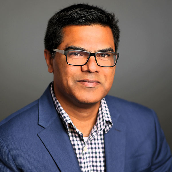
Shiva Rai
Director of Technology, Compound Semiconductors and Photonics, Applied Materials
Bio:
Shiva Rai is part of Applied Materials, the leading semiconductor OEM. In his current role, he leads the technology development for compound semiconductors and photonics applications. He also drives strategic initiatives with eco-system partners in these fields to help accelerate the technology development.
Prior to this, he held various technical lead roles in the photonics industry. At Bridgelux, an LED lighting manufacturer, Shiva has led the product design, development and strategy of their successful Vesta Series Tunable White LED platform. He held diverse LED manufacturing and R&D positions at Lumileds both in their Blue and Red LEDs for automotive applications. Prior to that, Shiva served as the CTO of a solar startup company, Izar Solar, developing III-V dilute-nitride based multi junction solar cell technology. During this time, he was successful in demonstrating a technologically viable solution for a multi junction dilute III-V solar cells on Si that could bridge the performance gap between commercial Si solar cells and specialty III-V Solar cells.
Shiva holds a PhD in Electrical Engineering from University of South Carolina (GaN HEMTs) and an MBA from Arizona State University. His technical expertise and current areas of focus are in photonic devices (physics, design, process & packaging) and Compound semi based RF & power devices.
Abstract:
Artificial Intelligence is reshaping every industry, economy and even geo-politics. At the heart of the AI are the key semiconductor technologies like GPUs, HPC, HBM and heterogeneous integration, that enables the growth in AI. As with any growth story, there is always a question about sustainability of that growth. The tasks that AI undertakes using these advanced semiconductor chips demands orders of magnitude higher power from the current infrastructure. This is a formidable challenge to the energy industry demanding innovations across the supply chain - from utilities all the way to datacenter operations. This challenge is providing unprecedented opportunities for innovations in new materials, devices and system architectures. Applied Materials is actively participating in many aspects of these innovations with the goal to not only help bring new technologies to market but also to scale them to high-volume-manufacturing.

