ABOUT THE EVENT
The semiconductor industry is at the center of the technological advances transforming society. It is an exciting time rich with opportunities to make a positive impact on your future products and tomorrow’s world.
Join global semiconductor-industry executives, opinion leaders, and decision makers in redefining what it means to develop fair, sustainable, and trusted technologies—and come away with deep tech solutions for your future products.
This three-day event will offer inspiring keynotes, solutions-oriented conferences, an exhibition showcasing the latest demos and startups, plus business meetings and focused networking, all in one place and all designed to bring you maximum value.
CTO, GlobalFoundries
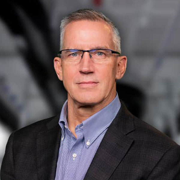
Bio:
Gregg Bartlett is Chief Technology Officer for GF, a position he was appointed to in 2022. He leads the execution and delivery of the company’s differentiated technology roadmap, including partnering with key universities and institutions to drive innovation, and accelerating development and delivery of GF’s differentiated technology. Mr. Bartlett oversees technology development, design enablement, GF Labs and global reliability and technology solutions.
Prior to his current role, Mr. Bartlett was Senior Vice President of Technology, Engineering and Quality at GF from 2019 to 2022. Before that, he served in various senior executive roles at GF including Head of Technology Development, Chief Technology Officer and Head of the CMOS (complementary metal-oxide-semiconductor) business from 2009 to 2019. Before joining GF, Mr. Bartlett spent 25 years in technical and management positions at Freescale Semiconductor and its predecessor, Semiconductor Products Sector at Motorola. Mr. Bartlett currently serves as a member of the board directors of Carbice Corporation.
Mr. Bartlett holds a bachelor’s degree in Chemical Engineering from Kansas State University.
Abstract:
The IoT/Edge Compute Era has ushered in an order of magnitude increase in connected devices each year compared to
smart mobile devices. With this comes great challenges in processing data at the edge with connected devices, the need
for intelligence and security in those devices, all with an eye toward sustainability. These formidable challenges create great
opportunities for innovation. For semiconductor foundries, this is the first compute era not dominated by single digit
nanometer technology, rather by creating compelling features on existing technologies to enable this connected, intelligent
and power efficient ecosystem. Building that ecosystem requires great R&D partnerships to deliver on the promise of this
future world
CTO, Stellantis
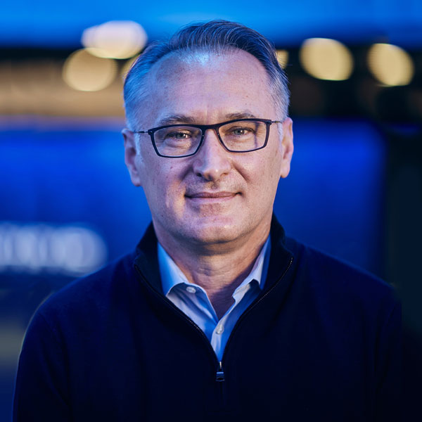
Bio:
Ned Curic was appointed Chief Technology Officer and a member of Stellantis’ Top Executive Team on August 30, 2021. From June 2017, Ned Curic was Vice President, Alexa Automotive at Amazon spearheading Amazon’s efforts in the Automotive industry. Ned Curic started his career in 1996 in the field of Engineering Systems at Northrop Grumman, an American multinational aerospace and defense technology company. After a short stint in the financial industry, in 2000 he joined Microsoft where he held various roles in Consulting, Product, Security and Advisory. He entered the automotive sector in 2013, as Group Vice President & Chief Technology Officer at Toyota Motor North America and, in 2015, became Co-founder and Executive Vice-President, Technical Director and Board Member at Toyota Connected. Ned Curic studied Informatics and Computer Science, and received a Master’s in Business Administration (Pepperdine University, George L. Graziadio School of Business and Management) in 2012.
Abstract:
Technologies have the power to reshape the auto industry, change the way we experience mobility and, ultimately, transform our life and our society. In guiding this transformation, we need to make sure that we don’t develop tech for tech’s sake but rather a tech made for real people, designed around their needs, delightful and easy to enjoy, whose impact is also fair, respectful of the environment and sustainable.
CEO, Intel

Bio:
Patrick (Pat) Gelsinger is chief executive officer of Intel Corporation and serves on its board of directors. He has more than four decades of technology leadership and experience driving innovation, with 30 of those years serving in Intel engineering and executive roles.
Before rejoining Intel in February 2021, Gelsinger was CEO of VMware. In that role, he transformed VMware into a recognized global leader in cloud infrastructure, enterprise mobility and cybersecurity – almost tripling the company’s annual revenues. Gelsinger was also ranked the top CEO in America in 2019 in Glassdoor’s annual employee survey. Prior to joining VMware in 2012, Gelsinger was president and chief operating officer of EMC’s Information Infrastructure Products business, overseeing engineering and operations for information storage, data computing, backup and recovery, RSA security and enterprise solutions.
Gelsinger began his career in 1979 at Intel, becoming its first chief technology officer and serving as senior vice president and the general manager of the Digital Enterprise Group. He managed the creation of key industry technologies like USB and Wi-Fi. He was the architect of the original 80486 processor, led 14 microprocessor programs and played key roles in the Intel® Core™ and Intel® Xeon® processor families, leading to Intel becoming the world’s preeminent microprocessor supplier.
Gelsinger earned degrees in electrical engineering: an associate degree from Lincoln Technical Institute, a bachelor’s degree from Santa Clara University and a master’s degree from Stanford University. He was elected a member of the National Academy of Engineering in February 2023. Gelsinger holds eight patents in the areas of VLSI design, computer architecture and communications, is an IEEE Fellow, and serves as a member of the National Security Telecommunications Advisory Committee. He also sits on the Business Council, Business Roundtable, CEO Council, CEO Forum, Global Semi Alliance, Tech Council CEO and U.S. Chamber China Center Advisory Board.
Chief Science Officer, Google X
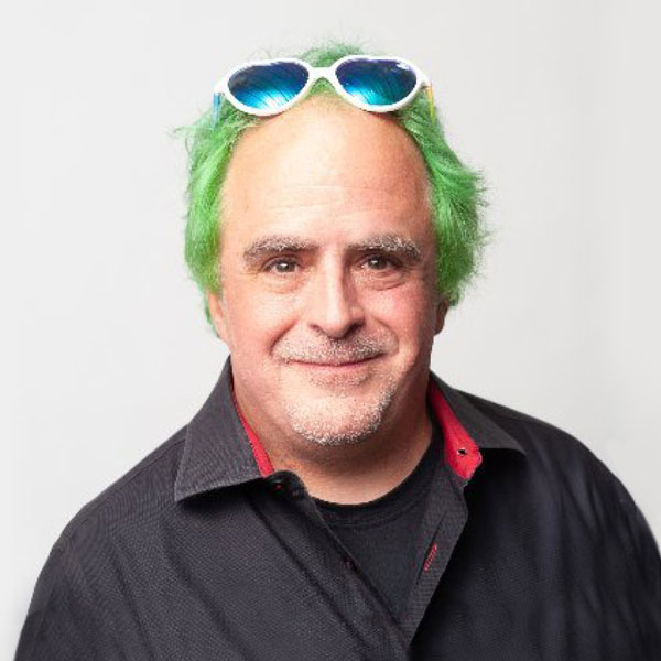
Bio:
Dave is a scientist, inventor, and entrepreneur whose work emphasizes the role of machine learning and AI, especially with respect to time-series data, search and optimization in program space, and decision making under uncertainty. He is Chief Science Officer at X and runs a team of mathematicians and machine learning experts working on early stage projects. He co-founded several companies, including Cerebellum Capital, which was an asset management company powered by an auto-ML system that discovered trading strategies. He also invested in and advised a number of startups in the data science and wearables space. He previously worked at Bodymedia, where he ran the machine learning team and several advanced development projects. Over the years, he’s helped start a number of other businesses. Personally, he’s a husband, father, snowboarder, passionate player of soccer and bridge, a puzzle nerd, a burner, and a travel-lover. He runs robot & programming clubs for his two kids to help them & friends get a deeper tech education. He got started down his path at Stanford University (1994: BS Symbolic Systems, BA Psychology) and completed his official education at UC Berkeley (2003: PhD EECS with a focus on Artificial Intelligence). He feels very lucky to have been interested in AI & ML well before it was cool.
Abstract:
The field of artificial intelligence is changing at a breakneck pace, revolutionizing many industries along the way, including software engineering and many elements of artistic creation. In addition to briefly introducing X (formerly Google X), this talk will discuss these trends and implications for hardware design, both in terms of how AI can fit into the design process as well as what changes could supercharge these coming applications.
GM IBM Semiconductors & VP Hybrid Cloud Research, IBM
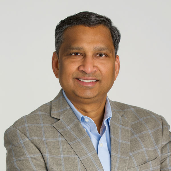
Bio:
Dr. Mukesh V. Khare is General Manager of IBM Semiconductors division and Vice President of Hybrid Cloud research. He leads a global team of more than 1000 researchers and engineers that are re-defining the future of computing for next generation workloads such as generative artificial intelligence (AI), high-performance computing, and their delivery via hybrid multi cloud. His research agenda includes semiconductor process technology, chip design for accelerated computing, system architecture and hybrid cloud software. Throughout his career, Dr. Khare has built and driven collaborative research alliances that lead to breakthrough advances in computing, such as 7nm and 2nm chip technologies. In 2019, he championed the formation of the AI Hardware Center, a $2.3B initiative to drive innovations in AI hardware technologies through public-private partnerships.
He serves on the Board of the Semiconductor Research Corporation (SRC), which manages more than $100 million in funding for university research in the fields of semiconductors. He is also a member of key academic boards such as Purdue and the State University of New York where he focuses on helping to build the semiconductor industry workforce. In 2021, Mukesh was the recipient of the Asian American Executive of the year award for his vision and execution of breakthrough nanotechnology. Dr. Khare served as the General Chair of the 2018 Symposia on VLSI Technology, has co-authored more than 100 research papers and holds many U.S. and international patents.
Dr. Khare is a recipient of an IBM Corporate Award, IBM’s highest technical award for his leadership in delivering innovative technologies and is also an IBM Distinguished Engineer. He holds a Master of Technology from IIT Bombay and a Doctorate in Electrical Engineering from Yale University. He is a strong advocate of diversity and inclusion in the workplace, and sponsors initiatives such as PowerUp for women engineers.
Abstract:
The potential of generative AI to radically change how we work and live has sparked our collective imagination. These new models can improve productivity through helping us write better code, give us a better customer service experience, or even help to discover new drug therapies. Just last month at Think 2023, IBM announced watsonx, our full stack approach to providing enterprises with an end-to-end solution for building, tuning, and deploying generative AI solutions. At the foundation of this stack, IBM is building AI infrastructure optimized for complex AI workloads. In this talk, we will discuss how IBM Research is powering this infrastructure, touching on our Vela supercomputer and our Artificial Intelligence Unit (AIU) based AI System One. We will also cover our roadmap for AI hardware innovation, fueled by what’s next in semiconductor technology.
Director IT Div., METI
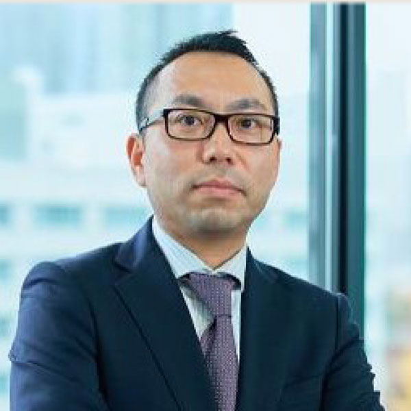
Bio:
He entered to the Ministry of International Trade and Industry in 1998. He was a visiting fellow at Stanford University and received his MBA from EDHEC Business School.
He has successively hold the positions at Industrial Revitalization Division, Economic and Industrial Policy Bereau and at Policy Planning and Coordination Division, Minister's Secretariat since 2009.
He also has experienced the positions of Director of Japan's Economic Revitalization Secretariat, Cabinet Sectetariat, as well as Deputy Commissioner of Los Angeles Office, Japan External Trade Organization, and Director of Industry Creation Policy Division, Economic and Industrial Policy Bureau, etc., since 2014. He has been on his current position since July 2022.
Abstract:
The environment surrounding the digital industry, digital infrastructure and the semiconductors they are based on is facing significant changes. These include the advance of digitalization due to COVID-19 responses, the moves toward carbon neutrality by 2050, tight supply/demand conditions of semiconductors worldwide, trade issues surrounding cutting-edge semiconductors and digital technologies, and economic security.
In this presentation, the strategy of Japan's semiconductor industry recognizing these changes, including enhancement of basic semiconductor production capacity, technology development for beyond 2nm next generation semiconductor will be presented.
Chairman of the Board of Directors, Rapidus Corp
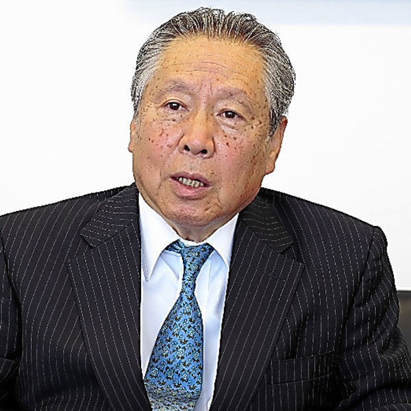
Bio:
TETSURO HIGASHI is the first Chairman of the Board of Directors at Rapidus Corporation, a company that researches, develops, designs, manufactures, and sells advanced logic semiconductors, in August 2022.
Prior to this role, Higashi had held a series of executive roles at Tokyo Electron Limited from 1990 until 2019 when he resigned from his position at the company. After his experience as Vice President at the company’s Motorola Sales Department and the Diffusion Systems Department, and General Manager at the SPE 2 Division, he had joined the executive board as Corporate Director in 1990. Following that, he was appointed to President and CEO of the company starting from 1996 when he was 46 years old. He had become Chairman of the Board in 2003 and reappointed as President and CEO in a dual role in 2013. In 2016, he had was appointed Corporate Advisor and resigned from his position at the company in 2019.
Mr. Higashi holds senior positions at several organizations related to semiconductor and technology including Directors Emeritus of SEMI (Semiconductor Equipment and Materials International) since 2012, Advisor of SEAJ (Semiconductor Equipment Association of Japan) since 2016, and Chairperson of the Executive Board of TIA since 2017. In addition, he was appointed to Chairman of Leading-edge Semiconductor Technology Center (LSTC), an organization that conducts next-generation semiconductor research, in 2023.
Mr. Higashi was born on August 28, 1949, in Tokyo, Japan and received a B.A. (1973) in Social Science from International Christian University and a M.A. (1977) in Social Science from Tokyo Metropolitan University.
Abstract:
At first, talk about the historical change in the world of regional semiconductor market share and its meaning, and then raise the issue why leading-edge semiconductor technology becomes so critical and vital for national security and economy. Lastly overview the role and mission of “Rapidus” and “LSTC” which represent the Leading-edge Semiconductor Technology Center in Japan.
EVP & Power Systems and Services, Schneider Electric
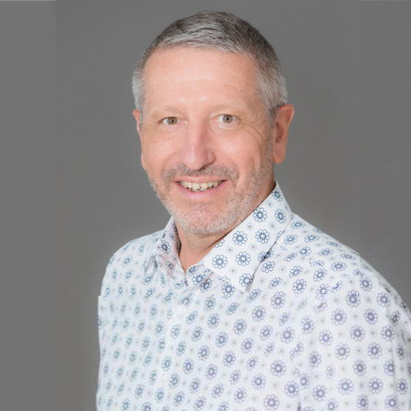
Bio:
Frederic Godemel joined Schneider Electric in 1990. Since then, his career has developed mostly around the power business in both low and medium voltage. Frederic has held operational functions in France, China and more recently in Dubai, he is now back in France. He was appointed Executive VP for Global Field Services back in 2018, EVP for Power Systems in January 2019 and more recently in July 2020 Executive VP for Power Systems and Services. Frederic is participating in speaking and panel opportunities on behalf of Schneider Electric, the most recent were TAQA in Abu Dhabi, TSIA in Orlando, CERA Week Houston and Reuters London. Frederic graduated from the Ecole Centrale Nantes in electrical engineering and holds an MBA from ESSEC Business School.
Abstract:
A more electric and digital world, which we call Electricity 4.0, is key to addressing the climate and energy crises and unocking a sustainable and resilient future. Electricity is the most efficient energy and the best vector of decarbonization, and with digital innovation it unleashes huge potential to eliminate energy waste. Only by disrupting the way we manage energy can we deliver a net zero carbon world.
The semiconductor industry also has the responsibility to transform its energy use for a net-zero future. The good news is that semiconductor companies have made many commitments to decarbonize their operations, especially their fabs. But how are they delivering on their green promises?
Join this inspiring talk from energy and automation leader Schneider Electric to explore the value of digital energy technology and meaningful partnerships that help ensure a bright and sustainable future for semiconductor companies.
Senior Director of Technology, HP

Bio:
Agnieszka has over 23 years of digital transformation and product innovation experience. Recognized as a thought leader in emerging technologies and trends, she has a strong track record of managing and aligning global high performance multicultural teams to deliver strategic value.
Over the past 16 years she has held multiple technical and management roles across HP businesses. As Senior Engineering Director, she drove the delivery of full stack software on devices and to Enterprise customers. As Head of Innovation Partnerships, she gathered and led cross-industry, multidisciplinary research experts to create open collaboration models that unleashed impactful innovation. Her breadth of knowledge ranges from electronics and communication systems to digital manufacturing and complex cyber-physical architectures.
Fluent in four languages, she holds a MSc in Communication Systems Engineering from the University of the Basque Country in Spain.
CEO, Soitec
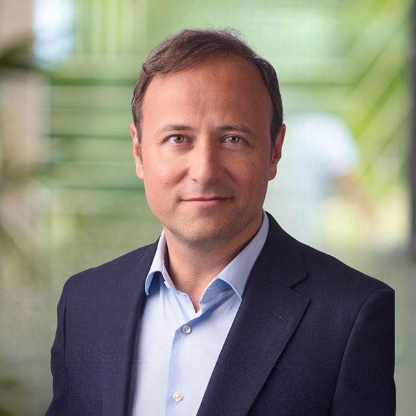
Bio:
Pierre Barnabé was nominated as Soitec CEO in January 2022 and joined the company four months later.
He was previously Executive Vice-President in charge of Big Data & Cybersecurity at technology group Atos (2015-2021), where he also led the Public Sector & Defense division and manufacturing operations before serving as interim Group CEO in 2021.
Prior to its acquisition by Atos in 2014, Pierre Barnabé was Deputy CEO of Bull. He then served as Bull’s Chairman & CEO from 2015 to 2021, spearheading the company’s evolution into a global leader in cybersecurity services and supercomputing.
From 2011 to 2013, he was Managing Director of the Enterprise branch of SFR, the French telecoms operator, where he launched cloud computing and very high-speed broadband activities.
That followed a 13-year stint during which he held various positions at Alcatel and Alcatel-Lucent, first in sales and later as Chairman & Managing Director of Alcatel-Lucent France (formerly Alcatel CIT) and Group Deputy Managing Director for Human Resources and Transformation.
A graduate of the NEOMA Business School and Ecole Centrale in Paris, Pierre Barnabé began his career in 1994 in Silicon Valley, developing corporate venture capital and capital risk activities for Thales Group. He then moved to Thales headquarters in Paris, where he was in charge of strategy and acquisitions for the Communication and Command division.
A member of the board of the multinational market firm Ipsos, he also served as Chairman of the Board of ENSIMAG Grenoble, the prestigious Grande École specializing in computer science, applied mathematics and telecommunications (2016-2022) and on the board of France’s National Institute for Research in Digital Science and Technology (INRIA) from 2021 to 2022. Pierre Barnabé is a Knight of the French National Order of Merit.
CEO, Lam Research
Bio:
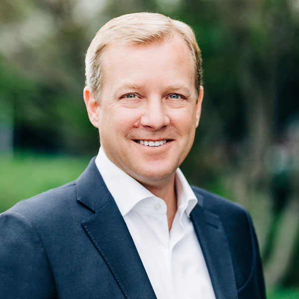
Timothy M. Archer is president and chief executive officer at Lam Research. During his tenure as CEO, he has driven revenue growth of more than 50%* and an EPS increase of more than 85%*. He joined the company in 2012 following its acquisition of Novellus Systems, Inc. (“Novellus”) when he began serving as Lam’s executive vice president and chief operating officer. He was later promoted to president and chief operating officer, and then president and chief executive officer in December 2018.
Tim currently serves on the International Board of Directors for SEMI, the global industry association representing the electronics manufacturing and design supply chain. From 2020 to 2022, he served as chairman of the board for the National Consortium for Graduate Engineering Degrees for Minorities (GEM): a nonprofit organization in the U.S. that is dedicated to increasing the participation of underrepresented groups in engineering and science at the master’s and doctoral levels.
Prior to joining Lam, Tim had an 18-year tenure at Novellus where he served as the company’s COO, and held other executive positions supporting worldwide sales, marketing, customer satisfaction, and product and business development. He began his career at Tektronix, Inc. in 1989, developing processes for high-speed bipolar integrated circuits.
Tim completed the Program for Management Development at the Harvard Graduate School of Business and earned his B.S. degree in applied physics from the California Institute of Technology.
*Calendar year 2018 compared to calendar year 2021
Abstract:
Increasing speed and scale to deliver on the future of specialty technologies.
Specialty technologies are ubiquitous – an essential connection between our physical and digital worlds. Poised to play an even bigger role in how we live and interact every day, it’s critical to accelerate device development and improve high volume manufacturing. However, as one of the most technically and geographically fragmented market segments, achieving greater speed and scale is challenging. It’s time to leverage the latest innovations including more advanced, application specific tools, virtual process development, and Equipment Intelligent® capabilities in the specialty technologies market to deliver on the future of a smaller, more connected world.
Group VP Technology, STMicroelectronics
Bio:
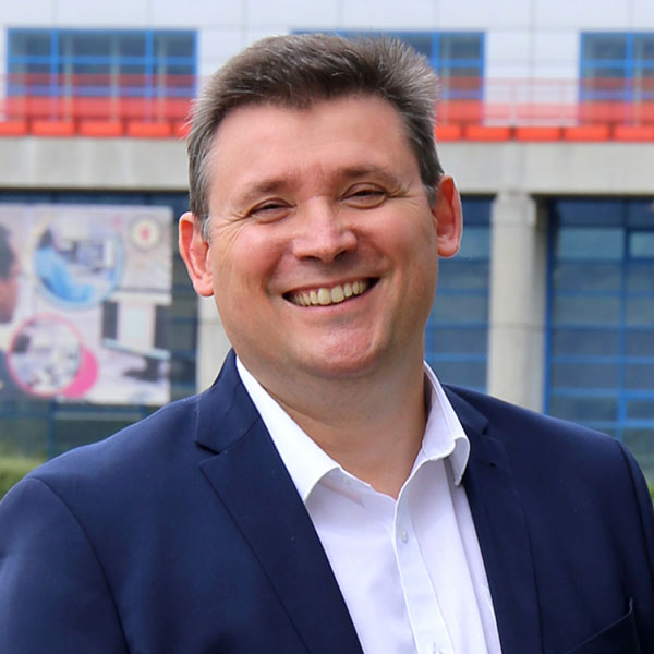
Since 2024, Serge Nicoleau is Group Vice-President Technology in charge of defining, implementing, and driving the R&D governance of Digital and BCD technologies of STMicroelectronics. He started his career in STMicroelectronics in 1998 in manufacturing management of the 200mm Crolles fab, nearby Grenoble. After various positions in manufacturing, process engineering, equipment engineering, he joined in 2004 the Crolles 300mm fab within the Crolles2 Alliance between STMicroelectronics, Motorola/Freescale and Philips/NXP. In 2007, he became Director of Industrial Technologies, before enlarging his responsibilities in 2012 as Deputy Director of the Operations of both Crolles 200 and 300 fabs.
This role included a specific responsibility for the industrial challenges of Automotive and IoT products in technologies ranging from 0.5μm down to 28nm critical dimensions with their multiple variants and options. In 2018, Serge Nicoleau is engaged into the new STMicroelectronics 300mm fab program in Agrate (Italy) to support Smart Power, Analog Mixed Signal and eNVM products. Then in 2020, he took the responsibility of the Technology & Design Platforms organization as General Manager. This organization is covering digital technologies, fast analog technologies, embedded memories, and optical sensors, with teams in France, in India, in United States which are addressing the digital products of STMicroelectronics.
Serge Nicoleau holds an Engineering Degree of the Ecole Polytechnique (Paris), a master’s degree in Theoretical Physics of the Ecole Normale Supérieure (Lyon) and a PhD in Particle Physics.
A three-day event
#LetiDays
The first “Modern Art & Gastronomy” reception at the Musée de Grenoble, privatized for the event, will feature a cocktail bar and cooking demonstration highlighting the region’s traditional ingredients, with musical entertainment by a violin duo. Don’t miss the guided tour (in English) of selected works.
The second reception, a “Garden Party à la française”, will be an outdoor affair at the historic Château de Sassenage against the breathtaking backdrop of the Vercors mountains. Step back in time during a tour led by period-costumed guides and dig into barbecue and local cheeses.
Function, company

Panel Session
Coming soon
Panel Session
Coming soon
VIDEO
Leti Innovation Days was back in 2023, with more than 1,000 people attending. Did you miss the event? Relive the highlights in video while you wait for the event to kick off!
CEA-Leti, a technology research institute at CEA, is a global leader in miniaturization technologies enabling smart, energy-efficient and secure solutions for industry.
For inquiries, please contact the event team at
or send us an email at [email protected]

© CEA-Leti. All rights reserved.

Ceci est un logo de sponsor

